

Solder Joint Integrity Test for Finding Latent Defects in PCBs
A novel method purports to locate defects that escape boundary scan and other tests.
Several test methods have been developed to find solder joint defects in printed circuit board assemblies. Capacitance method and IEEE 1149.1 or boundary scan are often used to find opens between component leads and pads on a board. These methods, however, only find complete opens or complete shorts.
Latent defects – ones that can develop after several years of field use – have not been found by conventional methods.
A new method to find such latent defects uses a 4-wire small resistance measurement technique built into a flying-probe in-circuit tester. It measures the resistance between component leads and pads, and checks the solder volume. Because solder volume is inversely proportional to the resistance in-between, the resistance measurement can be a way to test solderability.
Printed circuit board assemblies are tested several times following production. The tests are categorized as production test, board-level test and system test.1 Typically, automatic optical inspection is performed during production and used to not only check component placement but also monitor production yield (FIGURE 1).
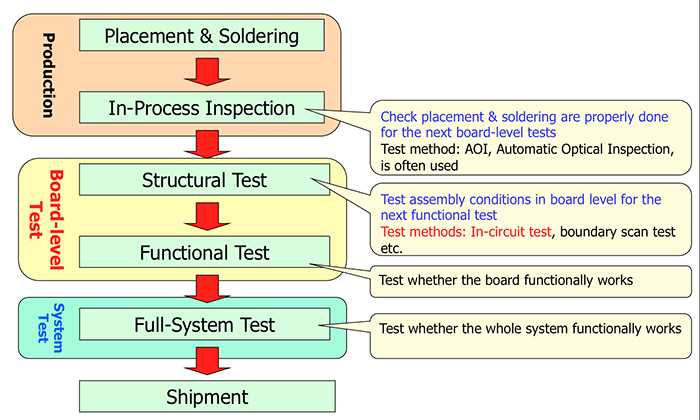
Figure 1. Typical PCBA test process.
The board-level test stage follows this in-process inspection. In this stage, board assemblies first are tested for structural integrity. Structural test is performed via in-circuit test or boundary scan, or both. Structural test, especially ICT, has another purpose. It works as a pre-check for the subsequent functional test. In functional test, power sources should be applied to the board assembly to be tested. Thus, if the board assembly is not structurally complete, it can be damaged during functional test.
Once board-level structural test is done, functional tests of board-level and system-level follow.
Carrying out all the tests incrementally increases test cost. Thus, in some cases, board-level tests are skipped, and only system test is performed. In an extreme case, manufacturers do not test their products at all. The decision to forego testing should be made carefully. It can result in massive incremental costs if defects are later found. Repair costs increase sharply as boards reach the shipment stage (FIGURE 2), a phenomenon known as the “10X rule in PWBA tests.”2
If a defective product comes to market, the problem will be much more serious. Consider the case of a car with a defective PCBA. A PCBA malfunction may cause an accident and injury. Once a defective board is distributed in the market, the recall cost could be one million times or more the original cost of the board.
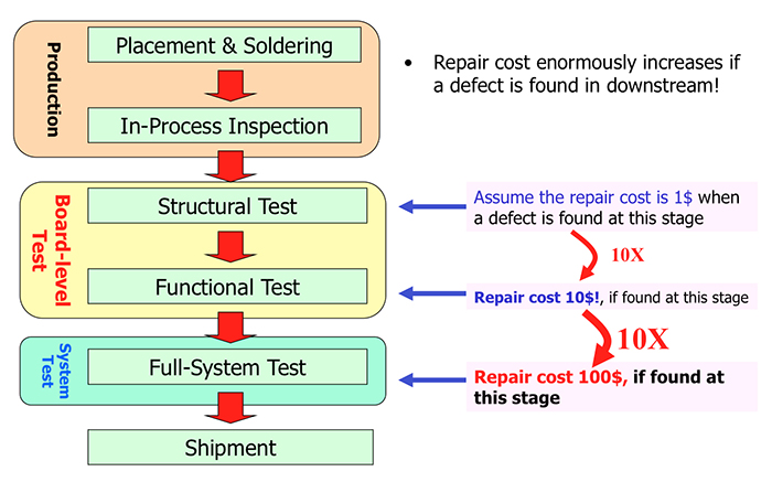
Figure 2. The 10X rule in PCBA test.
Clearly, manufacturers want to keep test costs as low as possible, but as noted, losses will ramp if the test strategy is wrong. To determine test strategy, the following two factors should be considered:
1. Quality. The required degree of test quality depends largely on the quality that the product needs. A cheap toy, for example, does not need board-level test. If it does not work at the system level functional test, it may be thrown away.
2. Volume. How many pieces will be produced is another important factor to determine test strategy. For small-volume production, the tester may not be required, but for high-volume manufacturing a dedicated tester and jigs may be required, lest the test process become a bottleneck.
Figure 3 shows examples of the relationships between product category and test strategy. The volume of automotive manufacturing is very high, but high quality is required as well.
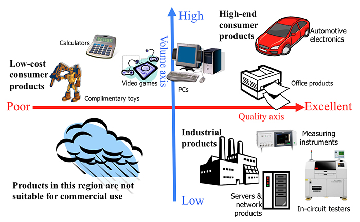
Figure 3. The relationship between product category and test strategy.
Defects that emerge after a board is delivered to customers are called latent defects. In automotive electronics, for example, latent defects may occur if a solder joint is not fully formed. When a car is in motion, the PCBA inside experiences vibration, and a solder joint either without solder or with insufficient solder may become completely open. Although there is not a failure during testing or initially in the field, the defect emerges after many hours in use.
Solder Joint Integrity Test (SJIT). The purpose of SJIT is to find latent defects. There are ways to find IC pin opens, but conventional capacitive, magnetic and diode methods cannot find latent pin opens. Boundary-scan test can locate IC pin opens but cannot find latent pin opens. X-ray tests can find latent pin opens but are too slow to test an entire board assembly.
The 4-wire resistance measurement method is a practical way to find latent defects (FIGURE 4). The lower the volume of solder, the higher its resistance becomes. Therefore, by measuring resistance across the solder joint, the reliability of that joint can be tested.
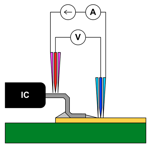
Figure 4. Solder joint integrity test, by 4-wire resistance measurement.
FIGURE 5 shows a schematic of the process. FIGURE 6 shows a finished solder joint. The resistance of the solder joint is 1.364mΩ. The resistance is defined as “PASS.” FIGURE 7 shows a poor solder joint with a resistance of 201.1mΩ. The test result is “FAIL,” for the resistance is more than 100 times the criterion.
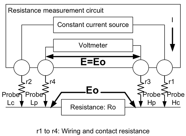
Figure 5. The electrical schematic of the SJIT.

Figure 6. A passing solder joint number.
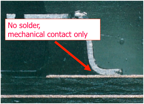
Figure 7. Failed solder joint number 1.
FIGURE 8 is another failed joint. The solder joint resistance is 3.969mΩ, about three times higher than the criterion. In FIGURE 9, another failure, the solder joint resistance is 63.45mΩ, about 16 times higher than the criterion.
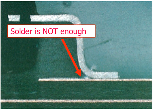
Figure 8. Failed solder joint number 2.
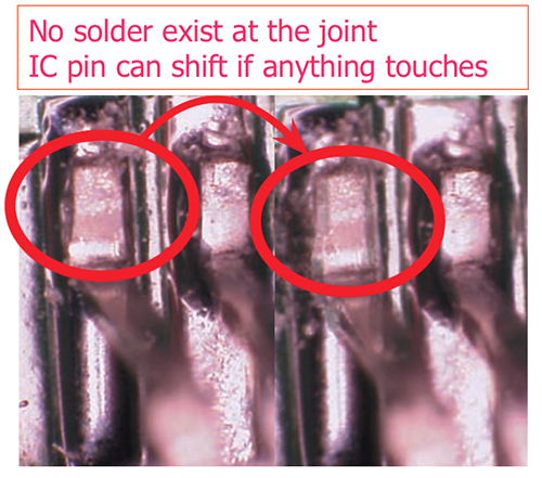
Figure 9. Failed solder joint number 3.
Conclusions
Repair costs increase dramatically if a defect is found in downstream. As such, manufacturers must screen out PCB defects in an early stage during structural tests. A defect found in the field could trigger recall costs of one million times or more the initial product cost, so during structural test at the assembler, potential latent defectives must be screened out as well.
The Solder Joint Integrity Test can be used to find latent defects, and the 4-wire resistance measurement method is the only way to find them at this time. Finally, this technique is industry proven; several manufacturing plants that produce assemblies for automotive applications have adapted it.
Ed.: This article was first published in the IPC Apex 2014 Proceedings and is reprinted here with permission of the author.
References
1. Hiroshi Yamakazi, “Key Drivers and Challenges for Electronics Packaging Test and Inspections,” The Japan Institute of Electronics Packaging, vol. 14, no. 1, 2011, pp. 26-30.
2 Koji Uchiyama, “Preparation for Test/Inspection Economical Scale,” The Japan Institute of Electronics Packaging, vol. 14, no. 2, 2011, pp. 103-108.
Hiroshi Yamazaki is assistant manager at Hioki E.E. Corp. (hioki.com); selmer@hioki.co.jp.


