

Updates in silicon and electronics technology.
Ed.: This is a special feature courtesy of Binghamton University.
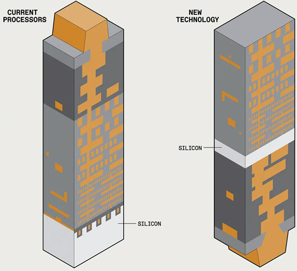
Next-gen chips will be powered from below. As transistors continue to be made thinner, the interconnects that supply them with current must be packed closer, which increases resistance and power. In processors, both signals and power reach the silicon from above. Arm researchers have developed a technology that separates those functions, saving power and making more room for signal routes. The signals travel along the copper traces of a PCB into a package that holds the SoC, through the solder balls that connect the chip to the package, and then via on-chip interconnects to the transistors. These interconnects are formed in layers called a stack. It can take a 10- to 20-layer stack to deliver power and data to the billions of transistors on today’s chips. (IEEC file #12450, IEEE Spectrum, 9/2/21)
Using liquid metal to turn motion into electricity, even underwater. North Carolina State University researchers have created a soft, stretchable device that converts movement into electricity and works in dry and wet environments. The heart of this energy harvester is a liquid metal alloy of gallium and indium. The alloy is encased in a hydrogel with the water containing dissolved salts (ions). The ions assemble at the surface of the metal, which induces a charge in the metal. Increasing the area of the metal provides more surface to attract a charge. This generates electricity, which is captured by a wire attached to the device. Researchers found that deforming the device by only a few millimeters generates a power density of approximately 0.5 mW/m-2, comparable to popular classes of energy harvesting technologies. (IEEC file #12449, Science Daily, 8/28/21)
Precision 2-D patterns could lead to next-generation electronics. Technical University of Denmark researchers have taken the art of patterning nanomaterials to the next level. This precise patterning of two-dimensional (2-D) materials offers a novel route to next-generation computation and storage, which can deliver better performance and much lower power consumption. One of the most significant recent discoveries within physics and material technology is 2-D materials such as graphene. Graphene is stronger, smoother, lighter and better at conducting heat and electricity than any other known material. But perhaps the most distinct feature of 2-D materials is their programmability. The properties of these materials can be dramatically changed by creating delicate patterns in them. (IEEC file #12492, Materials Today, 9/24/21)

Researchers develop woven lithium-ion batteries. Fudan University researchers have developed high-performing woven lithium-ion fiber batteries that can be woven into textiles and other materials. While such fiber batteries have been produced previously, it was thought that this type of battery internal resistance is too great to be used as a practical power source. The team showed the resistance of such fibers is not linear and instead follows a hyperbolic cotangent function relationship, meaning the internal resistance of such batteries levels off as battery length increases. The battery fibers have an energy density of 85.69WHr/kg, which is significantly higher than standard fiber batteries. The fibers are constructed by depositing lithium manganate particles onto carbon nanotubes, separated from a silicone-coated carbon nanotube sheet via a gel electrolyte. (IEEC file #12451, Electropages, 9/2/21)
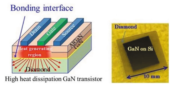
Add the speed of GaN to the thermal conductivity of diamond. Osaka City University researchers have bonded gallium nitride to a diamond substrate at room temperature and demonstrated the bond can withstand heat treatments of 1,000°C, making it ideal for the high-temperature fabrication process of GaN-based devices. Attempts have been made to create a GaN-on-diamond, using some form of transition or adhesion layer, but the additional layer interfered with thermal conductivity. High-temperature (500°C) direct wafer bonding was a possibility, but thermal mismatch cracked the bonded result. The answer was “surface-activated bonding” (SAB) atomically cleaning and activating the surfaces so they react when brought into contact with each other. This technique is a route to high-performance power semiconductors. (IEEC file #12457, Electronics Weekly, 9/9/21)
New optical “transistor” to speed computation up to 1,000 times, at lowest switching energy possible. Skoltech and IBM researchers have created an extremely energy-efficient optical switch that could replace electronic transistors in a new generation of computers manipulating photons rather than electrons. In addition to direct power saving, the switch requires no cooling and is really fast. At 1 trillion operations per second, it is between 100 and 1,000 times faster than today’s top-notch commercial transistors. The new switch conveniently works at room temperature and therefore circumvents all these problems. The switch could act as a component that links devices by shuttling data between them in the form of optical signals. It can also serve as an amplifier, boosting the intensity of an incoming laser beam by a factor of up to 23,000. (IEEC file #12479, Semiconductor Digest, 9/22/21)
In-situ diagnosis of solder joint failure by means of thermal resistance measurement. It is very important to develop a reliable method to detect cracks in solder joints. When a solder joint cracks, parts of the solder are replaced by air gaps, leading to an increase of the thermal resistance. As a result, the detection of the changes of the thermal resistance could give the information of crack ratio in the solder joint. Tokyo Institute of Technology researchers have developed a nondestructive and in-situ crack detection method based on the measurement of thermal resistance. This study indicates the thermal resistance from heat source to cooling plate of a sample will not only be affected by crack ratio but also the crack’s relative location and the heat source. The relationship between thermal resistance and crack ratio of a given solder area is examined experimentally and numerically on FET samples with different solder areas. (IEEC file #12473, Microelectronics Reliability, 8/1/21)
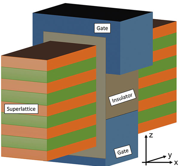
Technology for downscaling transistors could advance semiconductor design. Purdue University researchers have developed “Cascade Field Effect Transistor” (CasFET) technology, which could help design transistors that are smaller, use less power and switch from on to off at smaller applied voltages. Hence, this could lead to better and more powerful central processing unit generations, which can compute more operations with less energy. The key aspect is the superlattice perpendicular to the transistor’s transport direction, which permits switchable cascade states. CasFET does not require band-to-band tunneling, so designers are able to develop faster-switching and more energy-efficient transistors. (IEEC file #12472, Semiconductor Digest, 9/20/21)
Compact amplifier could revolutionize optical communication. Chalmers University researchers have developed a unique optical amplifier expected to revolutionize both space and fiber communication. The new amplifier offers high performance and is compact enough to integrate into a chip millimeters in size and does not generate excess noise. The new amplifiers offer a level of performance high enough that they can be placed more sparingly, making them a more cost-effective option. They work in a continuous wave (CW) operation rather than only a pulsed operation. The technology is useful in a range of applications, such as space communication and in fiberoptic cables. (IEEC file #12475, Science Daily, 9/21/21)
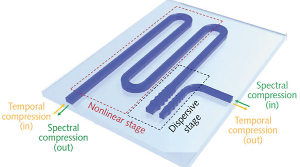
Higher signal processing possible by ultra-strong squeezing of light. Singapore University of Technology researchers have developed a temporal compression system that demonstrates the ability to squeeze light in time by a 11-fold compression of light in time could prompt a crucial paradigm for light generation in advanced metrology, imaging, and high-speed optical communications. The system permits an equivalent increase in the number of bits transmitted by light in a fiberoptic network. It provides orders-of-magnitudes smaller footprint than existing benchtop com used for generating short pulses in ultrafast optical signal processing. The two-stage design features a dispersive element and nonlinear component integrated on the same chip providing high compression. (IEEC file #12477, Laser Focus World, 9/22/21)
Market Trends
3-D nano-inks push industry boundaries. Michigan Technological University researchers have created a way to make a 3D-printable nanocomposite polymeric ink that uses carbon nanotubes (CNTs). This revolutionary ink could replace epoxies in additive manufacturing and is more versatile and efficient than casting. Adding low-dimensional nanomaterials such as CNTs, graphene, metal nanoparticles and quantum dots permits 3-D-printed materials to adapt to external stimuli, giving them features such as electrical and thermal conductance, magnetism, and electrochemical storage. What they have done differently is use polymer nanocomposites and a printing process that doesn’t sacrifice functionality. (IEEC file #12486, Science Daily, 9/24/21)
Integrated electronics trends to drive IME market to $1.5 billion by 2032. In-mold electronics (IME) enables electronic functionality to be embedded within molded and thermoformed plastic components. With the integration of capacitive touch, lighting, and even haptics, along with size and weight reductions of up to 70%, IME is an efficient approach to making curved touch-sensitive interfaces. IDTechEx forecasts IME to be a $1.5 billion market by 2032, with applications mainly within the automotive and consumer sectors. Greater integration of electronics within 3D structures is an ever-increasing trend, representing a more sophisticated solution compared to the current approach of encasing rigid PCBs. IME facilitates this trend by enabling multiple integrated functionalities to be incorporated into components with thermoformed 3-D surfaces. (IEEC file #12484, Printed Electronics World, 9/22/21)
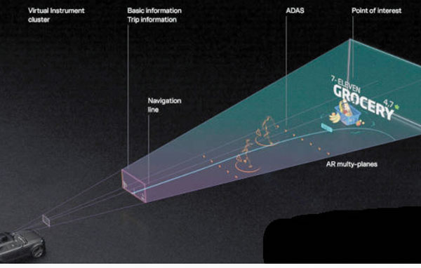
Holographic windscreen enables in-car head-up display. WayRay has developed an automotive heads-up augmented reality display that uses a large part of the windscreen, and positions virtual objects at different apparent distances. It turns the entire windshield into a virtual world where information about the vehicle, navigation, infotainment, and the surroundings can be shown while blending with the real world. Its red-green-blue lasers are mounted remotely and connected by optical fiber to a “picture-generating unit” from which light travels in free space to the windscreen. Inside the windscreen are functional layers including a holographic polymer film. The concept is to display different types of information at different apparent depths, from dashboard-type data in the near-field, to the vehicle’s ADAS-proposed travel path stretching into the far distance, highlighting real objects of interest seen through the windscreen. (IEEC file #12461, Electronics Weekly, 9/7/21)
Solar cells with 30-year lifetimes for power-generating windows. University of Michigan researchers have developed a transparency-friendly solar cell design that could marry high efficiencies with 30-year estimated lifetimes, which may pave the way for windows that also provide solar power. These devices, used on windows, turn a building into a power plant. While silicon remains king for solar panel efficiency, it isn’t transparent. For window-friendly solar panels, researchers have been exploring organic materials. These materials are known generally as “non-fullerene acceptors” to set them apart from the more robust but less efficient “fullerene acceptors” made of nanoscale carbon mesh. The team has already increased the transparency of the module to 40%, and they believe they can approach 60%. (IEEC file #12468, Science Daily, 9/14/21)
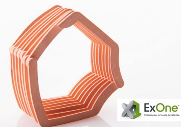
3-D-printed copper windings for electric motors. ExOne and Maxxwell Motors researchers have successfully proved a new concept for 3-D printing a high-efficiency copper e-winding design for electric motors using a binder jet system. The new process eliminates many of the challenges that come with traditional manufacturing of copper coils for electric motors. In binder jetting, machines bond layers of metal powder with a binding agent before final sintering in a furnace. The technology excels at making complex metal parts with excellent mechanical properties. (IEEC file #12481, Design Fax, 9/17/21)
Market for fully printed sensors will reach $4.9 billion by 2032. Printed and flexible sensors constitute the largest printed electronics market outside of displays, and the market for fully printed sensors will reach $4.9 billion by 2032. This growth is despite the sustained displacement of its largest market: printed glucose test strips. Market growth of the overall category is enabled by the rise of many new applications. Printed sensors span a diverse range of technologies and applications, ranging from image sensors to wearable electrodes. Each sensor category seeks to offer a distinctive value proposition over the incumbent technology, with distinct technological and commercial challenges on route to widespread adoption. Most important is the increasing adoption of IoT and Industry 4.0 because they will require extensive networks of often wirelessly connected low-cost and unobtrusive sensors. (IEEC file #12482, Printed Electronics World, 9/15/21)
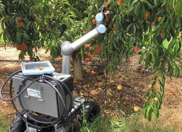
Intelligent robots pick, prune in the peach orchard. Georgia farmers produce 130 million pounds of peaches every year. Workers around the orchard are tasked with pruning, thinning, and picking. Georgia Tech Research Institute researchers are testing a new idea to have a robot do all three. They developed an intelligent robot using AI and sophisticated navigation to handle the tasks of removing branches, finding good peaches, and removing them from a tree. The robot uses both LIDAR and GPS to self-navigate through the orchard. The LIDAR system determines distances by targeting an object with a laser and measuring the laser beam’s return time, while the GPS measures locations. (IEEC file #12483, NASA Tech Briefs, 9/21/21)
Recent Patents
Electrical interconnect structure with radial spokes for improved solder void control (assignee: Infineon Tech.) patent. no. 20210233839. An electrical interconnect structure includes a bond pad having a substantially planar bonding surface, and a solder enhancing structure that is disposed on the bonding surface and includes a plurality of raised spokes that are each elevated from the bonding surface. Each of the raised spokes has a lower wettability relative to a liquefied solder material than the bonding surface. Each of the raised spokes extend radially outward from a center of the solder enhancing structure.
Filled through silicon vias for semiconductor packages (assignee: Semiconductor Components Industries) patent. no. 11,075,306. Implementations of semiconductor packages may include a wafer having a first side and a second side, a solder pad coupled to the first side of the wafer, a through silicon via (TSV) extending from the second side of the wafer to the solder pad, a metal layer around the walls of the TSV, and a low melting temperature solder in the TSV. The low melting temperature solder may also be coupled to the metal layer. The low melting temperature solder may couple to the solder pad through an opening in a base layer metal of the solder pad.
Printed circuit board assemblies with engineered thermal paths (assignee: Anaren Inc.) patent. no. 20210243880. A printed circuit board (PCB) having an engineered thermal path and a method of manufacturing are disclosed. In one aspect, the PCB includes complementary cavities formed on opposite sides of the PCB. The complementary cavities are in a thermal communication and/or an electrical communication to form the engineered thermal path, and each cavity is filled with a thermally conductive material to provide a thermal pathway for circuits and components of the PCB. The method of manufacturing may further include drilling and/or milling each cavity and filling the cavities.
Package substrates with magnetic buildup layers (assignee: Intel Corp.) patent. no.11081434. The present disclosure is directed to systems and methods for improving the impedance matching of semiconductor package substrates by incorporating one or more magnetic buildup layers proximate relatively large diameter, relatively high capacitance, conductive pads formed on the lower surface of the semiconductor package substrate. The one or more magnetic layers may be formed using a magnetic buildup material deposited on the lower surface of the semiconductor package substrate. Vias conductively coupling the conductive pads to bump pads on the upper surface of the semiconductor package substrate pass through and are at least partially surrounded by the magnetic buildup material.
Chip-last wafer-level fan-out with optical fiber alignment structure (assignee: Ayar Labs) patent. no. US2021 /018049. A redistribution layer is formed on a carrier wafer. A cavity is formed within the redistribution layer. An electro-optical die is flip-chip connected to the redistribution layer. A plurality of optical fiber alignment structures within the electro-optical die is positioned over and exposed to the cavity. Mold compound material is disposed over the redistribution layer and the electro-optical die. A residual kerf region of the electro-optical die interfaces with the redistribution layer to prevent mold compound material from entering the optical fiber alignment structures and the cavity. The carrier wafer is removed from the redistribution layer.
PCB to dielectric layer transition w/controlled impedance and reduced crosstalk for quantum (assignee: IBM Corp.) patent no. 11102879. A transition between a printed circuit board (PCB) and a dielectric layer with controlled impedance and reduced and/or mitigated crosstalk for quantum applications are provided. A quantum device can comprise a microwave quantum circuit on a dielectric substrate and a PCB comprising a via that comprises a transmission line. A wirebond between the transmission line of the PCB and a transmission line of the microwave quantum circuit operatively couples the microwave quantum circuit to the PCB. The via comprises a defined characteristic impedance. The wirebond provides a microwave signal connection between the PCB and microwave quantum circuit.
Printed wiring board islands for connecting chip packages (assignee: Intel Corp.) patent no.11,134,573. A printed wiring board island relieves added complexity to a printed circuit board. The printed wiring board island creates an island form factor in the printed circuit board. Coupling of a semiconductive device package to the printed wiring board island includes a ball-grid array. The ball-grid array can at least partially penetrate the printed wiring board island.
is technology analyst at IEEC, Binghamton University. He has over 40 years’ experience in electronic packaging. He previously was the chief mechanical engineer at Lockheed Martin; gmiller@binghamton.edu.
The Integrated Electronics Engineering Center (IEEC)at Binghamton University is a New York Center of Advanced Technology (CAT) responsible for the advancement of electronics packaging. Its mission is to provide research into electronics packaging to enhance our partners’ products, improve reliability and understand why parts fail. Research thrusts are in 2.5/3-D packaging, automotive and harsh environments, bioelectronics, flexible and additive electronics, materials for packaging and energy storage, MEMS, photonics, power electronics, sensors, embedded electronics, and thermal challenges in electronic packaging. More information is available at binghamton.edu/ieec.
Does sustained ISO 9001 and Lean Six Sigma deliver success?
Sustaining quality management systems and continuous improvement strategies is critical for retaining a competitive advantage in the printed circuit board industry. Implementing and sustaining both ISO 9001 and Lean Six Sigma provides quality improvements, enhances organizational performance, creates efficiencies, increases market share, improves financial performance, and reduces product reliability risk. This quantitative correlational study evaluates critical success factors for implementing and sustaining ISO 9001 and Lean Six Sigma. Survey data were collected from the North American printed circuit board (PCB) industry. Canonical correlations were used for data analysis. A statistical correlation was found between critical success factors for implementing and sustaining ISO 9001 and Lean Six Sigma. Three canonical variates were extracted and interpreted.
Quality has become a key process indicator for manufacturing and service companies. Quality is a strategic priority for all modern businesses.1 Improving and sustaining quality is a critical organizational strategy to retain customers in today’s globally competitive environment. Quality management is used to proactively find solutions to current and future cost and risk problems.
To continue reading, please log in or register using the link in the upper right corner of the page.
An interview with Colombia’s largest EMS company.
Colombia is the 28th largest country by population and the 38th largest by nominal GDP. Residing as South America’s connection into Central America, it is in the same time zone as the Eastern US during daylight saving time.
Invertronica was founded in early 2003 in Colombia and includes several companies involved in the design, prototyping and manufacturing of electronics products. Those companies include Tecrea, an electronics design and engineering unit; LosComponentes.com.co, a parts distributor, and Colcircuitos, the largest EMS company in Colombia. It can move fast: 24 hours from design to assembly.
To continue reading, please log in or register using the link in the upper right corner of the page.
A look back at friends and colleagues who left us in 2021.

Semi genius - Akasaki
Isamu Akasaki, 92, Japanese physicist invented the first efficient blue LED and shared the 2014 Nobel Prize in physics.
Robert “Bobby” Baker, 60, Sanmina/SCI senior buyer.
To continue reading, please log in or register using the link in the upper right corner of the page.
A new study reveals emerging applications for attaching very-fine-pitch parts using low-temp methods.
Electrically conductive adhesives (ECAs) have been touted for decades as a potential replacement for solder. Technology roadmaps by organizations ranging from IPC to the Surface Mount Council often listed ECAs as a “coming” technology, and scores of papers have been presented highlighting possible uses and likely end-products.
In early October, the international research firm IDTechEx released a new study called “Electrically Conductive Adhesives 2022-2032: Technologies, Markets, and Forecasts.” Matthew Dyson, Ph.D., a senior technology analyst at IDTechEx specializing in printed, organic and flexible electronics, spoke with Mike Buetow about the study’s findings.
To continue reading, please log in or register using the link in the upper right corner of the page.
By concentrating heat onto the part, the BGA avoids excessive temperature.
Recently, a customer asked if we could remove a valuable BGA from an existing circuit card assembly. About 1,000 of these BGAs could be removed. Our customer is a reclamation company, and they planned to resell the BGAs, which could fetch upwards of $400 each because of the current chip shortage.
The BGA itself is an older version of the Intel Altera family of products (FIGURE 1). While deemed obsolete by the manufacturer, the part is certainly usable, and due to the chip shortage, our customer might understandably obtain a good price for these older parts, which can be used as replacements for newer models.
To continue reading, please log in or register using the link in the upper right corner of the page.

Press Releases
- Parmi Expands Mid-Atlantic Sales Coverage with Cope Assembly Products
- Seika Machinery to Host SMI 2026 Webinar Series Session 2 on PCB Slicing Methods and Low-Stress Separation
- Pillarhouse USA Expands BarTron, Inc. Sales Territory into Indiana
- Mycronic appoints Peter Andries as General Manager of MRSI Systems and VP of Global Technologies Division