

2014 Articles
“DFRM” reveals potential manufacturing issues and the sample of processes that can feed those issues back for design review.
As detailed in CIRCUITS ASSEMBLY last year (“Robotics Assembly from Prototype to Production,” March 2013), robotics has received an increase of attention in the media thanks to overall advances in the technology.1 This article details some of the key areas of design for robotics manufacturing (DFRM), and provides recommendations for products transitioning from the design to production phase.
During the prototype or design verification build stage, the main goal is to prove out the bill of materials (BoM), assembly drawings and overall robotics design. This is the phase when manufacturing issues are documented and fed back for resolution before a product is released to production.
The following are examples of areas of focus during the prototype review:
Form, fit and function. Two validations exist during the form, fit and function stage. First is a design review of the build documentation, including design models, BoM and assembly drawings. Depending on tools available, the review could be electronically automated or manual, with the result a validation that the overall build documentation meets the intended design intent. The second validation is the actual assembly of the robot and how all the material fits together. Problems may occur with sheet metal, plastic material or wire routing interference issues. Wire routing may require additional review, given the opportunity of pinching, wires unplugging or other reliability concerns. If any of these issues occur, an engineering change order (ECO) may be required to the design model and assembly drawings.
Rework or modification to material may be required to make the prototype “fit” together. As with any modification, an increased attention should be made on the impact to the next-level assembly. The important takeaway of this rework is to incorporate a permanent correction into the next assembly build or product roadmap. Issues may also occur during revision changes of a dimension modification. The goal is to verify the fit, modify if necessary and address and incorporate all changes before the follow-up build or before the introduction-to-production phase.
During the design and build review, consider analysis tools such as PFMEA (Process, Failure, Mode, Effects and Analysis) or equivalent to assess areas of the process in which error proofing (Poka yoke) tools or methods can be used. The PFMEA review can look at materials, methods, process and equipment. Similar analysis can be completed during the initial design stage (DFMEA - Design, Failure, Mode, Effects and Analysis). These reviews assess the areas at risk, categorize and prioritize the risk, and determine what can be implemented to prevent the issue from occurring. Typically, this exercise is completed with a cross-functional team to ensure a variety of backgrounds, experiences and knowledge, which ensures a comprehensive assessment is performed.
Ease of manufacturing. Following the DfM process after the form, fit, function review, ease of manufacturing is assessed. Ease of manufacturing identifies ways to reduce product cycle time and improper quality. These ideas range from the simple to the complex. Examples include using captive washer screws or pre-applied adhesive verses hand-applying adhesive. Another example is having multiple wires or cables harnessed together for ease of routing and assembly.
In addition to changes in material, correct selection of equipment and tooling can greatly help the ease of manufacturing. If an assembly has many screws at the same operation and torque setting, an electric or automated screw driver may assist. An assessment may be required to justify the expense or return on investment of the purchase. Custom designed fixturing may be the most helpful of all ease-of-manufacturing recommendations. These fixtures may assist with product support, various assembly operations (such as press-fit), material handling and inspection. Figure 1 shows an example of a custom fixture, designed and manufactured at Benchmark Electronics NH Division for a medical robotics program. Some of the benefits of this custom fixture include reduced process cycle time and increased product quality through better material handling.
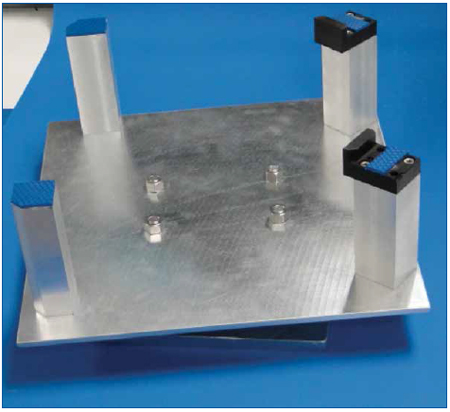
Figure 1. Custom designed turntable fixture for ease of manufacturing. (Courtesy Benchmark Electronics NH Division)
Quality control and test review. As discussed above, the initial design build is an important DfM review tool to ensure form, fit and function of a robotics assembly. Two additional important inputs result from quality control and testing of the subassemblies and completed robotics assembly. These two inputs will also be fed back to the DfM review as potential design change for future builds.
During quality control or visual inspection, among the items reviewed include adherence to internal and external criteria, industry standards and potential areas of concern for functionality of the subassemblies. Cosmetics issues will also be reviewed for the completed robot, usually focusing on external surfaces visible to the end-customer.
Depending on the end-application, various noise levels such as fans, motors and gears may be an area of DfM feedback.
The acceptable noise level for a robot in an industrial or military application may be quite different from one in a medical or office environment.
Figure 2 shows an example of a gear system. In cases of motors and gears, testing feedback through the subassembly and final robotics system test will impact DfM review. Testing will verify design, functionality and application with a complete load placed upon the assembly. Be aware of the noise and overall decibel level and consider the final customer application and environment.
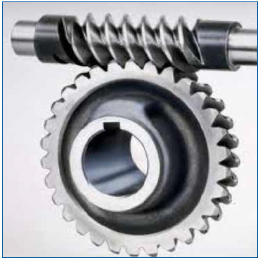
Figure 2. Sample gear system. (Courtesy howstuffworks.com)
References
1. Scott Mazur, “Robotics Assembly from Prototype to Production,” CIRCUITS ASSEMBLY, March 2013.
Scott Mazur is manufacturing staff engineer at Benchmark Electronics (bench.com); scott.mazur@bench.com.
How Aqueous Technologies is leading the way toward clean assemblies.
It all started, fittingly, on a napkin.
Below the San Bernardino Mountains in Rancho Cucamonga, CA, you’ll find Aqueous Technologies, a cleaning company launched more than 20 years ago. The manufacturer of cleaning systems for electronics assemblies is the vision of Mike Konrad, president and CEO.
Konrad, described by colleagues as having “a special entrepreneurial spirit,” saw “water as the future” of cleaning boards when he started in a garage in Northern California. It was in that garage that Konrad designed his first cleaning machine, outlining it in pen on a napkin. That makeshift parchment now resides, in a frame, at the current company headquarters.
Konrad was at the time working for a soldering equipment manufacturer. It was the 1989 signing of the Montreal Protocol, which eventually banned CFCs, then the primary cleaning solvent for printed circuit boards, that inspired him to launch Aqueous Technologies. “There was considerable concern, even panic as there was no real (legitimate) alternative,” recalled Konrad in an interview.
“At that time, there were water-based cleaners, but they were little more than mildly converted dishwashers and were better at soliciting jokes than cleaning boards.” Still, the basic technology behind these water-based cleaners had promise.
Konrad suggested the development of a water-based alternative to solvent cleaners, but his employer wasn’t interested. Funding the startup himself, Konrad and a friend designed a water-based cleaning system, which they sold to his employer. Emboldened, he began developing designs for systems that would be more environmentally safe, including a zero-discharge cleaning system, which, he says, had no impact on the environment. That’s where his employer balked and Konrad walked.
“When I approached my employer with that idea, they were not impressed. Seeing no need, they rejected my idea. With necessity being the mother of invention, and rejection being the mother of motivation, I resigned and started my own company.”
Aqueous moved into its current Rancho Cucamonga, CA, location six years ago, but the 15,000 sq. ft. facility still looks brand new. In January, CIRCUITS ASSEMBLY toured the facility with national sales manager John Hall, who has been with the company for nine years.
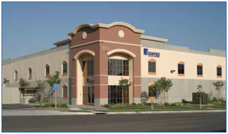
Figure 1. Aqueous Techologies’ current headquarters in Rancho Cucamonga, CA.
All around the facility, there is an extended family feel. “I started working on the assembly line in college just to pay for a trip to Ireland and Scotland,” Hall recalled. Today, Hall is not only one of the firm’s 30 staffers, 28 of whom work onsite, he is also Konrad’s son-in-law. Almost all of them are in production, and 80% of the building is designated for manufacturing.
Aqueous believes its single-minded approach is an advantage. “Our only focus is cleaning machines,” Hall said, giving Aqueous “the luxury of putting more thought into the machines” to become “more and more environmentally conscious.”
Perhaps that’s why Aqueous boasts the biggest market share in the US for batch machines, the only type of washer the company designs and builds. Given that the assembly market has trended away from inline equipment, competitors have taken notice. “Every inline manufacturer, without exception, has built a batch cleaner in the last few years,” asserts Hall.
The facility is a testament to the industry’s response. In one conference room stands a glass case that houses more than 40 industry awards (including multiple Circuits Assembly New Product Introduction Awards). Across the hall is a cleaning and analysis demo site for customer samples, where clients can “dial in” on what they need before buying a machine, Hall explains.
The demo room includes a cleaner, a tester and visual analysis. The company’s flagship Trident cleaner and defluxer is designed to remove all flux types from an assembly, according to Hall, and to do so in any mode of discharge: full, low or (the most popular) zero. Like its customers, Aqueous is “conscientious about how much water, power and chemicals we use and how we dispose of them,” says Hall.
The Trident machine reuses water and holds onto the chemicals. “Aqueous cleaners are designed not to go into the drain. Our zero-discharge systems filter and re-deionize solution and rinse water to alleviate draining requirements.
“Flux conducts electricity. We remove flux at the end so voltage only goes where you want it to go. Flux allows dendrites to grow, so we remove them,” said Hall. “How clean a board needs to be depends on where it’s going. How long does it have to be in the field?”
Besides the napkin, the site contains other nods to the past. Hall points out the Zero-Ion G3 cleanliness tester in the showroom, an updated version of the machine originally developed in the 1970s in the US Navy. Designed to indicate assembly cleanliness, the system also takes quick, accurate measurements on bare boards and other electromechanical devices. Aqueous still sells the machine today.
Also in the showroom are a microscope and camera. Residues that cannot be seen visually are subject to a ROSE (resistivity of solvent extract) tester. Roughly one in three boards is sent out to special labs such as Foresite in Indiana, ACI Technologies in Philadelphia, or one of Trace Labs’ sites for ion chromatography testing. The labs can determine “‘where and what’ is on the boards before we set up a cleaning process,” said Hall.
In the building’s main manufacturing area resides a raw stainless steel weld shop. After welding, a newly built machine is powder-coated to protect the frame.
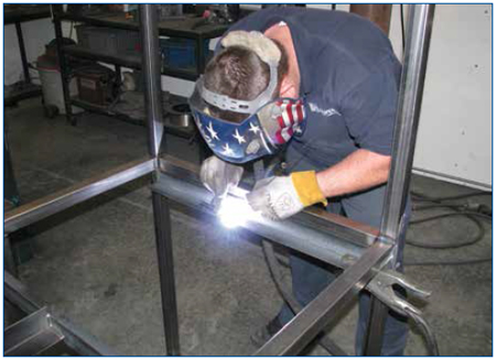
Figure 2. All Aqueous’ machines start from a common frame and take about a month to build.
Aqueous builds all its machines from a common dishwasher frame purchased from an outside party (which Hall did not disclose). All the parts are removed from inside the frame, the most cost-effective option, and half are donated to a local engineering school. The dishwasher frames are “stamped stainless. There are no openings,” Hall says.
During the build process, parts are kitted and then inserted into the machine. Once it gets to the kitting stage, “from frame to chamber to everything in it” takes a couple days. The whole process of building a machine takes about a month. The Trident machine includes tanks, pumps, a blowing system, and resistivity probes, and it runs on a Windows touch-screen platform.
‘Designed for Anyone’
In practice, users first create a cleanliness profile, including cleanliness level, wash time, wash temperature, rinse time, dry time, dry temperature, chemical concentration, and then, since it is all preprogrammed, “the operator just has to hit start and stop.”
The manufacturing floor also contains an Eco-cycler machine, which, according to the company, “captures, filters, re-deionizes, and reuses rinse water from defluxing systems.” In short, it makes everything zero-discharge.
Hall says Aqueous embraces the so-called “dishwasher stigma.” The proof is industry acceptance, he points out. The type of equipment Aqueous builds has been legitimized because “every company has one,” he says.
Hall was visibly excited when asked about upcoming new products. At IPC Apex Expo in Las Vegas this month, Aqueous is introducing two machines that Hall says will be the “next answer” to trends in cleaners for years. Usually, Hall said, the company only introduces small changes to the inside of current machines that are good for the end-user. He looks forward to unveiling brand new equipment.
“Demand for cleaning is definitely ramping,” he said. The primary end-markets are consumer, which is starting to ramp more, and military/biomedical, which has always cleaned. Hall adds, “It all comes from no-clean fluxes. Sometime in the last decade, the consumer side went to no-clean fluxes,” which have a lower solids content.
‘More Failures’
With the move to smaller parts, there is “more failure because of dendrite growth. Component miniaturization and lead-free cause higher reflow profiles.” Hence the “giant ramp” in cleaning, he said. This is also because of increased use of conformal coating, which has found its way into all sorts of non Class 3 product.
Aqueous does a lot of telecom work with firms such as Qualcomm, L3 Communications and contractors that work with these companies. Cellphones, for instance, are coated to protect the microphone from moisture, which often comes from the user’s own mouth. As Hall says, “To be good for adhesion, the board has to be clean.”
“Cleaning is a three-step process,” he said, referring to chemicals, rinsing and drying. “With lower surface tension, it’s easier to get into small spaces.” All of Aqueous’ efforts lie in the second step: rinsing, which involves large pumps, spray systems and nozzles. A specific type of nozzle is used at a certain angle to push chemicals out from under components.
Asked if cleaning chemistries are designed for types of boards, fluxes or specific machines, Hall replied, “All of the above.”
Don’t expect drop-in chemistry, however. Chemicals are formulated for different types of metal, alloys, flux, coatings, plastics, inks and labels, Hall explained. “Some chemicals work better in batch or inline worlds,” and “certain cleaning chemistries tend to work better with certain machines.” For low-standoff components, for instance, Aqueous recommends a “focused mechanical energy,” said Hall.
To keep up with the changes in cleaning trends and, especially, chemistry, Aqueous has formed strong relationships with other firms in the industry, including Zestron, Kyzen and Petroferm. “We listen for manufacturing process trends and adjust equipment designs based on information from our industry partners.”
They also teamed with other companies in the industry to host 16 education-based cleaning workshops in the past year alone. More are being lined up for this year.
Reaching out to industry seems a natural extension of the culture here. At Aqueous, there is a real sense of friendly, down-to-earth teamwork, all in pursuit of Konrad’s green dreams. At home, Konrad might be Hall’s father-in-law, but in the office, Konrad is seen not just as a boss and mentor, but as a visionary.
Today, Aqueous Technologies has built more than 4,000 washers. Those built just last year have saved more than 36 million gallons of water, Konrad says. “We set out to build an unapologetic legitimate cleaning machine that was environmentally responsible. I believe in doing so, we have made the world a slightly better place.”
Chelsey Drysdale is senior editor for PCD&F/CIRCUITS ASSEMBLY; cdrysdale@upmediagroup.com.
A new CAD tool imports design files and quantitatively predicts product life.
Previous approaches to reliability assurance included “gut feel,” empirical predictions such as MIL-HDBK-217 and TR-332, industry specifications, “lessons learned” programs, failure mode effects analysis, and test-in reliability schemes. While these approaches can provide some value, it is felt that the most comprehensive analysis can best be done virtually using computer modeling of the circuit board in the intended environment. Such modeling can predict the life and reveal any design weaknesses before any prototype boards are even built.
The motivation for using modeling software lies in ensuring sufficient product reliability. This is critical because markets are lost and gained over reliability. Reputations can persist for years or decades, and hundreds of millions of dollars are at stake.
Using an automotive example, some common costs of failure:
- Total warranty costs range from $75 to $700 per car.
- Failure rates for E/E systems in vehicles range from 1 to 5% in first year of operation (Hansen Report, April 2005).
- Difficult to introduce drive-by-wire, other system-critical components.
- E/E issues will result in increase in “walk home” events.
Other Costs of Failure Examples
Type of Business Lost Revenue/ Hour
Retail brokerages $6,450,000
Credit card sales authorization $2,600,000
Home shopping channels $113,750
Catalog Sales Centers $90,000
Airline reservation centers $89,500
Cellular service activations $41,000
Package shipping services $28,250
Online network connect fees $22,250
ATM service fees $14,500
Supermarkets $10,000
The foundation of a reliable product is a robust design. A robust design provides margin, mitigates risk from defects, and satisfies the customer. Assessing and ensuring reliability during the design phase maximizes return on investment. The cost associated with finding a design flaw increases greatly the longer it takes to find it. Some have estimated this cost to be:
- Found during design: 1x.
- Found during engineering: 10x.
- Found during production: 100x.
- Found at customer: 1000x.
Electronics OEMs that use design analysis tools hit development costs 82% more frequently, average 66% fewer respins and save up to $26,000 in respins.1
MTTF / MTBF. Many companies use mean time to failure or mean time between failures calculations as their only means of assessing the reliability of their product while in the design stage. MTTF applies to non-repairable items, while MTBF applies to repairable items. They are based on the exponential distribution:
- Distribution: F(t) = 1 – e-λt
- Density (pdf): f(t) = λ e-λt
- Survival (sf): S(t) = e-λt
- Failure rate: λ(t) = f(t) / S(t) = λ e-λt / e-λt = λ
- MTTF: = 1 / λ (mean time to failure)
MTBF is typically calculated through a parts count method. Every part in the design is assigned a failure rate. This failure rate may change with temperature or electrical stress, but not with time. Failure rates are summed and then inverted to provide MTBF. Most calculations assume single point of failure, while some calculations take into consideration parallel paths.
A variety of handbooks provide failure rate numbers. These include MIL-HDBK-217, Telcordia, PRISM, 217Plus, RDF 2000, IEC TR 62380, NSWC Mechanical, Chinese 299B, HRD5. Some companies use internally generated numbers.
MTBF/MTTF calculations tend to assume that failures are random in nature and provide no motivation for failure avoidance. And, it is very easy to manipulate numbers with tweaks made to reach desired MTBF, such as modifying quality factors for each component. These calculations are also frequently misinterpreted. Example: A 50,000 hr. MTBF does not mean no failures in 50,000 hr.; it means half the products could fail by 50,000 hr. Basically, these calculations are a better fit toward logistics and procurement, not failure avoidance. Furthermore, these calculations take into account only failure of the components on the board, not wear-out mechanisms such as solder joint failures, plated through-hole fatigue, or damage due to vibration or shock events.
Design-build-test-fix approach. A common approach to product development is the design-build-test-fix (DBTF) approach. This is essentially a trial-and-error approach where the product is designed and prototypes are built. These prototypes then undergo testing; failures/defects are discovered; corrections are made in the design, and more prototypes are made, etc. Traditional OEMs spend almost 75% of product development costs on this approach.2 Shortcomings of this approach include:
- All design issues often not well-defined.
- Early build methods do not match final processes.
- Testing doesn’t equal actual customer’s use.
- Improving fault detection catches more problems, but causes more rework.
- Problems found too late for effective corrective action, fixes often used.
- Testing more parts and more/longer tests “seen as only way” to increase reliability.
- Cannot afford time or money to test to high reliability.
Recommended Design Approach
To design a product with the best chance for optimal reliability, one must understand the primary wear-out mechanisms and failure modes (often referred to as physics of failure). These wear-out modes can then be modeled and avoided with proper design improvements. One must also understand the expected life of the product and environment that the product will be exposed to over the course of its life. Finally, state-of-the-art tools should be used to understand the design and its impact on reliability before prototypes are built (while product is still in the design stage).
Electronics failures are typically attributed to a quality defect, overstress or wear-out. Quality defects often result from mistakes made in manufacture of the component or in PCB assembly. Design for manufacture and Six Sigma quality controls are required to minimize such defects and are outside the scope of this article. Overstress failures occur when a product is used outside its intended purpose or is exposed to an environment for which it was not intended (example, dropping your iPhone in the commode). This mode of failure is also outside the scope of this article. Avoiding wear-out failures in an electronics product is the focus since these failure modes can be modeled using established algorithms.
Wear-out failures have become much more common with aggressive design practices to shrink the footprint of electronics and design-in more applications. This has led to smaller, more closely spaced solder joints and through-hole vias. IC packages also have lower standoff and thus exert higher stress on solder joints during thermal cycle excursions. Additionally, lead-free solders have been introduced, which require higher assembly temperature and have different mechanical properties.
The advantage of wear-out failures is that we can understand how these failures take place and model them. For example, one researcher found that 65% of electronic failures were due to thermo-mechanical effects (CTE differences or diffusion).3 Common wear-out failure mechanisms that are modeled with Sherlock modeling software include:
- Thermal-cycle fatigue of solder joints.
- Mechanical vibration failure of solder joints.
- Shock failure of solder joints.
- Plated through-hole fracture.
Understanding Product Environment
Desired lifetime and product performance metrics must be identified and documented. The desired lifetime might be defined as the warranty period or by the expectations of the customer. Some companies set reliability goals based on survivability, which is often bounded by confidence levels such as 95% reliability with 90% confidence over 15 years. The advantages of using survivability are that it helps set bounds on test time and sample size and does not assume a failure rate behavior (decreasing, increasing, steady-state).
If the environment in which the product will be shipped and used is understood, then these conditions can be inserted in the model, and their impact on wear-out failure can be calculated. Mechanical vibration and shock, as well as thermal excursions, during shipping can be estimated depending on how the product is transported. Some products require long storage times or aggressive storage conditions, and these can also be modeled. Of greatest concern is how the product is used by the customer. One must estimate the number and magnitude of temperature excursions and mechanical stresses that the product will be exposed to while in use.
Defining environments. Several commonly used approaches are used to identify the environment. One approach involves the use of industry/military specifications such as MIL-STD-810, MIL-HDBK-310, SAE J1211, IPC-SM-785, Telcordia GR3108, and IEC 60721-3. Advantages of this approach include the low cost of the standards, their comprehensive nature and consensus industry agreement. If information is missing from a given industry, simply consider standards from other industries.
Disadvantages include the age of the standards; some are more than 20 years old, and lack validation against current usage. The standards both overestimate and underestimate reliability by an unknown margin (Figure 1).
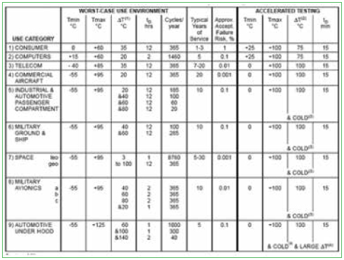
Figure 1. Some standards, such as IPC-SM-785, are too old to be inherently valid for today’s use.
Another approach to identifying the field environment is based on actual measurements of similar products in similar environments. This gives the ability to determine both average and realistic worst-case scenarios. All failure-inducing loads can be identified, and all environments, manufacturing, transportation, storage and field can be included.
In addition to thermal cycle environments, the reliability software accepts vibration and shock input as well. Figure 2 shows representation of this input. Identify the number of natural frequencies to look for within the desired frequency range. Single point or frequency sweep loading is available, and techniques are also available to equivalence random vibration to harmonic vibration.
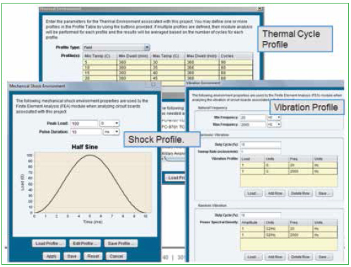
Figure 2. Environmental profiles inserted into software for modeling.
Vibration loads can be very complex and may consist of sinusoidal (g as function of frequency), random (g2/Hz as a function of frequency) and sine over/on random. Vibration loads can be multi-axis and damped or amplified depending on chassis/housing.
Transmissibility. The response of the electronics will be dependent on attachments and stiffeners. Peak loads can occur over a range of frequencies, including the standard range of 20 to 2000Hz and an ultrasonic cleaning range of 15 to 400kHz.
Vibration failures primarily occur when peak loads occur at similar frequencies as the natural frequency of the product or design. Some common natural frequencies:
- Larger boards, simply supported: 60 - 150Hz.
- Smaller boards, wedge locked: 200 - 500Hz.
- Gold wire bonds: 2kHz - 4kHz.
- Aluminum wire bonds: >10kHz.
Import files. The software is designed to accept ODB files, which contain all the data for the PCB, the components and their locations. Data can also be imported with Gerber files and an individual bill of materials (BoM). Figure 3 shows an example of a PCB stack-up and relevant data for reliability modeling.
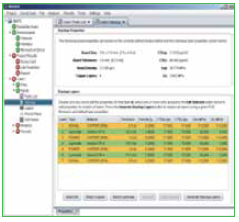
Figure 3. PCB layer viewer and relevant data.
Parts list. Individual component data is part of the ODB file; however, modifications to the data can be made manually to ensure physical characteristics of all the components are accurate. Figure 4 shows the component editor, and Figure 5 shows the laminates and their properties that are embedded in the software.
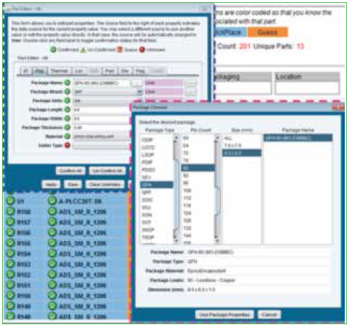
Figure 4. Parts list package database editor.
Analyses. Six analyses are currently conducted:
- CAF (conductive anodic filament) formation.
- PTH fatigue.
- Solder joint fatigue.
- Finite element simulations.
- Natural frequencies.
- Vibration fatigue.
- Mechanical shock.
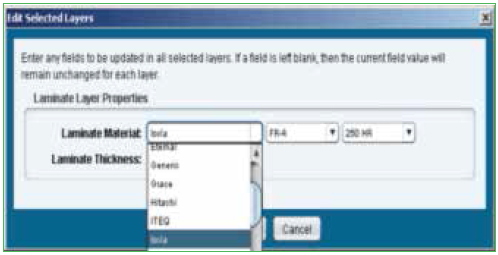
Figure 5. Laminate manufacturers.
CAF formation. Conductive anodic filament formation is when electrochemical migration of copper occurs between two barrel vias (Figure 6). The migration occurs through the PCB laminate and not on the surface (which is considered a different defect mechanism).
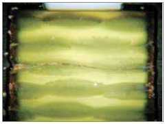
Figure 6. CAF formation between vias within the PCB.
One factor that drives CAF is damage to the laminate surrounding the drilled via. This can occur from a dull drill bit, excessive desmear etching or poorly laminated layers. Environmental factors that can increase the likelihood of CAF formation are the voltage across neighboring vias, spacing of the vias, and high temperature/humidity conditions. The software evaluates the edge-to-edge spacing of all the vias on the board and estimates the risk of CAF formation based on the damage around each via, as well as how well the product was qualified with CAF testing. Such vias can then be assessed to determine if there is a high voltage potential between them, or if they could be exposed to high humidity conditions.
PTH fatigue. PTH fatigue occurs when a PCB experiences thermal cycling. The expansion/contraction in the z-direction is much higher than that of the copper that makes up the barrel of the via. The glass fibers constrain the board in the x-y plane, but not through the thickness, so z-axis expansion can range from 40 to 70 ppm/°C. As a result, a great deal of stress can be built up in the copper via barrels, resulting in eventual cracking near the center of the barrel, as shown in the cross section photos in Figure 7.
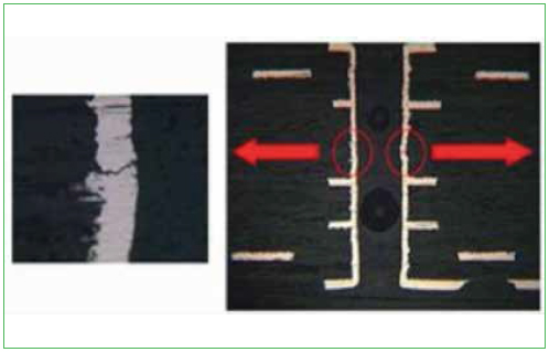
Figure 7. PTH fatigue images.
A validated industry failure model for PTH fatigue is available in IPC-TR-579, which is based on round-robin testing of 200,000 PTHs performed between 1986 and 1988. This model used hole diameters of 250µm to 500µm, board thicknesses of 0.75mm to 2.25mm and wall thicknesses of 20µm and 32µm. Advantages include the analytical nature in using a straightforward calculation that has been validated through testing.
Disadvantages include the lack of ownership and validation data that is approximately 20 years old. The model is unable to assess complex geometries, including PTH spacing and PTH pads that tend to extend lifetime. It is also difficult to assess the effect of multiple temperature cycles. However, this assessment can be performed using Miner’s Rule. The PTH equations take into account the expansion coefficient, PCB thickness, copper thickness, via diameter and glass transition temperature.
In addition to the series of algorithms used to calculate the fatigue life of PTHs, the quality of the copper plating is also taken into account. The “PTH Quality Factor” is a means of estimating the quality of the PTH fabrication process. This is a somewhat subjective determination. Rough edges of the copper wall will provide crack initiation sites and would reduce the quality. On the other hand, smooth copper walls, along with a surface finish such as ENIG, would improve the quality of the PTH. An example of a failure curve for PTH thermal cycle fatigue is shown in Figure 8, along with a list of vias in order of their expected life.
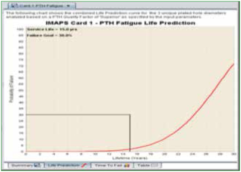
Figure 8. PTH fatigue life prediction.
Solder joint fatigue. Solder joint fatigue failures are becoming more prevalent due to the continued shrinkage of solder joint size and pitch that comes with more advanced packages. The reliability software takes into account the physical characteristics of the package and PCB to calculate thermal cycle fatigue life of the solder joints. The user may select eutectic tin-lead (SnPb), SAC 305 or SN100C (SnCuNiGe). Solder may be specified at the board or component level.
Solder Fatigue Model: Modified Engelmaier
The modified Engelmaier model is used within the software, which is a semi-empirical analytical approach using energy-based fatigue.
First, determine the strain range, Δγ, using:![]()
where C is a correction factor; LD is diagonal distance; a is CTE; ΔT is temperature cycle, and h is solder joint height. C is a function of activation energy, temperature and dwell time. LD is described further. Da is a2 – a1 and hs s defaults to 0.1016mm.
Next, determine the shear force applied to the solder joint using:![]()
where
F = shear force,
LD = length,
E = elastic modulus,
A = area,
h = thickness,
G = shear modulus, and
a = edge length of bond pad.
For the subscripts: 1 is the component; 2 is the board; s is the solder joint; c is the bond pad, and b is the board. This model takes into consideration foundation stiffness and both shear and axial loads. Leaded models include lead stiffness.
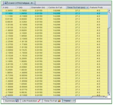
Figure 9. Tabular PTH fatigue life data.
Area. A1 is thickness of component (h1) x solder joint width, and A2 is thickness of board (h2) x solder joint width. As is length of solder joint (Ls) x solder joint width, which defaults to 45% of LD.
Ac is the length of the bond pad (Lc) x solder joint width. Lc defaults to 60% of LD.
Remaining parameters (h, G, v, a). Thickness: hs defaults to 0.1016mm, and hc defaults to 0.035mm.
Gs = Es / 2 x (1+vs) where Es = Temperature dependent modulus of solder and vs = 0.36.
Gc = Ec / 2 x (1 + vc) where Ec = 120 GPa and vc = 0.3.
Gb = Ec / 2 x (1 + vb) where Eb = 17 GPa and vb = 0.18.
a = √As.
Then, determine the strain energy dissipated by the solder joint using:
![]()
Calculate cycles-to-failure (N50), using energy-based fatigue models for SAC developed by Syed – Amkor:![]()
and using the energy-based model for SnPb
![]()
The software also has user overrides for solder fatigue.
Validation of Modeling Results
How accurate are the software’s modeling results compared with actual data? To answer this, more than 100 models were run with individual components and the results compared with reliability data from the literature. The results for QFNs, QFPs and BGAs are shown in Figure 10. The predicted results are on the x-axis and the modeled results on the y-axis. A perfect model would result in a diagonal line.
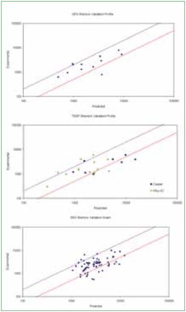
Figure 10. Predicted thermal cycle results compared with modeling results.
Naturally, there is variation in the results; however, for the most part, the predicted results are within a 10% band of the actual data. A larger
scatter in data is seen for BGAs, as is typical of experimental results for these components.
Unreliability. Thermal cycle results are provided as an unreliability plot that represents the cumulative reliability of all the components on the circuit card assembly (CCA) (Figure 11). The software will also show the rank order of individual components and their respective reliability so that the weakest links are determined (Figure 12). When a product consists of several CCAs, an unreliability failure plot is provided that takes into account all the assemblies.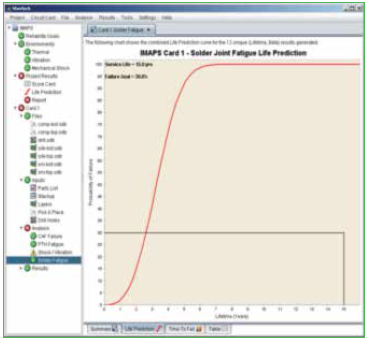
Figure 11. Solder joint fatigue life prediction (representing a very harsh under hood environment).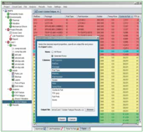
Figure 12. Sherlock results table.
Natural frequency analysis. The software contains an embedded finite element modeling tool that allows the user to select the mesh size and angle. The FEA is used to calculate the natural frequencies of the CCA, as well as the vibration and shock behavior. An example of the mesh created for a CCA is shown in Figure 13, followed by the first natural frequency generated for the assembly – based off the mount points used for the card.
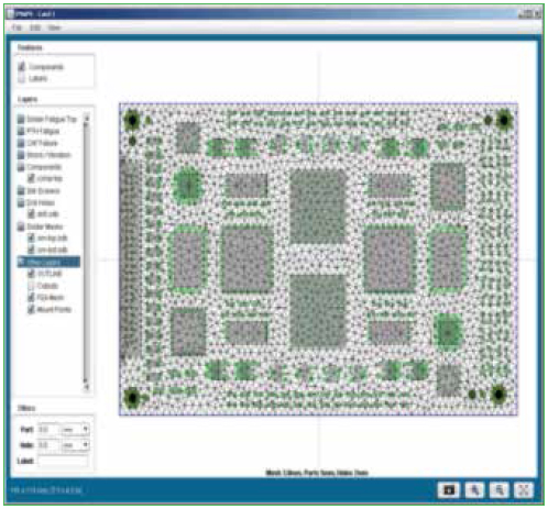
Figure 13. Mesh and mount points.
Vibration fatigue. Lifetime under mechanical cycling is divided into low cycle fatigue (LCF) and high cycle fatigue (HCF). LCF is driven by plastic strain and modeled by Coffin-Manson.
![]()
-0.5 < c < -0.7; 1.4 < -1/c > 2
HCF is driven by elastic strain and modeled by Basquin.![]()
-0.05 < b < -0.12; 8 > -1/b > 20
Vibration software implementation. The software uses the finite element results for board level strain in a modified Steinberg-like formula that substitutes the board level strain for deflection and computes cycles to failure. Critical strain for the component is defined by: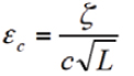
where
ζ is analogous to 0.00022B but modified for strain;
c is a component packaging constant (1 to 2.25), and
L is component length.
The Miles Equation relates Harmonic vibration to random vibration and must be utilized until the random vibration FEA code is fully tested and released.
![]()
where
fn = Natural frequency,
Q = transmissibility, and
ASDinput = Input spectral density in g2/Hz.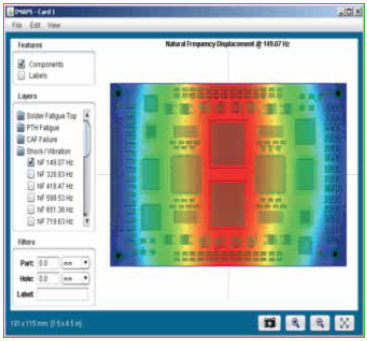
Figure 14. Natural frequency displacement.
The reliability software vibration modeling results show the displacement of the PCB at all locations (Figure 15). The results are plotted for each axis of vibration, and the most impacted components are revealed in the component list (Figure 16). Fatigue results are also shown in an unreliability plot over the life of the product, in the case where vibration is an ongoing event.
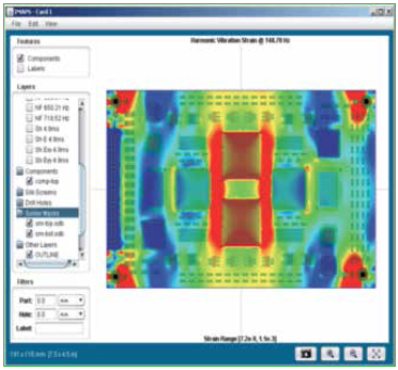
Figure 15. Graphical vibration results.
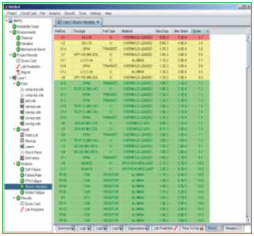
Figure 16. Graphical vibration results.
Mechanical Shock Environments
Mechanical shock requirements were initially driven by experiences during shipping and transportation. Shock became of increasing importance with the use of portable electronic devices and is a surprising concern for portable medical devices.
The basic environmental contributing factors include:
- Height or G levels.
- Surface (e.g., concrete).
- Orientation (corner or face; all orientations or worst-case).
- Number of drops.
JEDEC shock failure. Failures related to mechanical shock typically cause pad cratering (A,G in the image) and intermetallic fracture (B, F in Figure 17). This is an overstress failure, not a fatigue failure, and follows a random failure distribution.
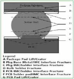
Figure 17. JESD22-B110A, Subassembly Mechanical Shock.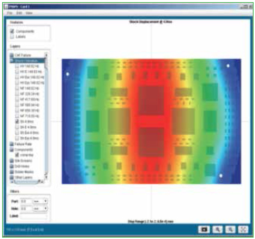
Figure 18. Shock displacement results for a test board.
The software analyzes shock based on a critical board level strain and will not predict how many drops to failure. Either the design is robust with regard to the expected shock environment, or it is not. Additional work has been initiated to investigate corner staking patterns and material influences. An example of the modeling showing displacement across a CCA after a shock event is shown in Figure 18. The rank order of components experiencing the largest strain is shown in Figure 19.
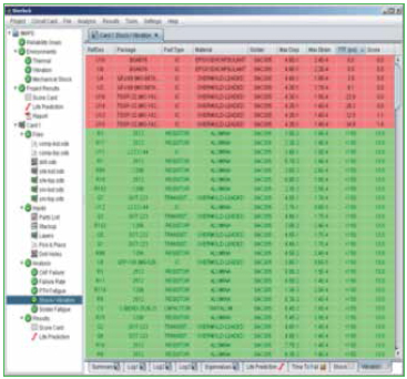
Figure 19. Components are listed in order of those experiencing the highest strain.
Constant failure rate module. A recent addition to the software has been the inclusion of a constant failure rate model using MIL-HNBK-217F calculations. Inputs necessary to compute failure rates are located in the parts list (Figure 20). The component failure rate is based off the 217F model and takes into account the temperatures at which the product operates. An example of the unreliability failure plot is shown in Figure 21, along with failure rates from solder joint fatigue and vibration.
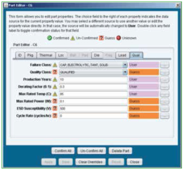
Figure 20. Failure rate information entry.
The appropriate test conditions can be determined by first generating a solder joint fatigue model based on the expected field conditions of the product. The percent failure at the required life is then known for the design. The model is then rerun using the desired thermal cycle test conditions (say 0° to 100°C). The number of cycles required to generate the same percent failure shown in the previous model is how many cycles are required (with no great percent failure). Naturally, the number of cycles may be increased if the sample size is reduced.
Early in the design phase of a product is the best time to run various what-if scenarios for the design. These might include experimenting to determine where the mount point locations should be in order to reduce strain on sensitive components. One may also run thermal cycling modeling using the various package options available for critical integrated circuits. The impact of changing a product from SnPb to Pb-free solder may also be evaluated.
Some high-reliability products require 100% ESS to ensure no poorly built products escape production. A common ESS test is thermal cycling; however, one does not wish to remove more than 5% of the useful life of the product during the ESS. By modeling the total life, it can be ensured that the number of cycles selected for ESS is appropriate.
Finally, many consumer electronics companies provide a warranty period for their products. Funds must be set aside for each product shipped to cover the expected field returns within the warranty period. It is important that these costs be roughly accurate and based on data, since money is lost if the retained amount is too large or too small. The results provided by the modeling tool can provide a portion of the total expected field returns due to hardware wear-out mechanisms.
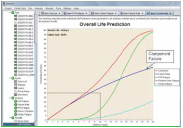
Figure 21. Life prediction that combines component failure with PTH and solder fatigue.
Summary
Designing in reliability upfront pays off immensely over the life of the product. To date, there has not been a simple-to-use method of estimating the wear-out life of an electronics product. The reliability software described here is designed to fill this need and does so by permitting rapid assessment of electronics systems reliability using physics of failure (PoF).
References
1. Aberdeen Group, “Printed Circuit Board Design Integrity: The Key to Successful PCB Development,” 2007.
2. Gene Allen and Rick Jarman, Collaborative R&D, John Wiley & Sons, 1999.
3. B. Wunderle and B. Michel, “Progress in Reliability Research in Micro and Nano Region,” Microelectronics and Reliability, vol. 46, no. 9-11, 2006.
Ed.: This article is adapted from a paper from SMTA International 2013 and is reprinted here with permission of the authors.
Dr. Randy Schueller is senior member of the technical staff at DfR Solutions (dfrsolutions.com); rschueller@dfrsolutions.com. Cheryl Tulkoff is senior member of the technical staff at DfR Solutions; ctulkoff@dfrsolutions.com.

Press Releases
- Adam Ryder appointed as Managing Director of Incap UK
- Metal Etch Services Opens New Motor City Facility to Meet Growing Midwest Demand
- Yamaha surface-mount line powers the future of specialized production at Inter-Company in Netherlands
- Matric Group Becomes the First U.S. Manufacturer to Deploy Panasonic NPM-GH Dual Lane SMT Technology