

2005 Articles
An All-Silicon Package?
It would permit the perfect match of identical materials. So, why not?
Wafer-level packaging is gaining momentum as newer designs and processes continue along the learning curve. Organic substrates, especially polyimide film (flex-based packaging), have achieved some level of success and continue to grow. Why not build an all-silicon package? Silicon joined to silicon would permit the perfect match of identical materials, enable efficient wafer-level processing and provide hermeticity in a chip-scale package.
Some might say that the flip chip is an all-silicon package, but is it really a package? And what about the organic underfill? A narrower definition of packaging requires reworkability, and once underfilled, a flip chip is not typically reworkable. While some progress has been made in reworkable underfills, removing and replacing a flip chip is not a factory-friendly process like reworking a standard SMD with only solder at the interface. Today’s flip chip really uses “post packaging,” as the underfill is applied by the assembler and is part of the packaging. And while most bumping is a wafer process, wafer-level underfill that is potentially more easily reworkable (thermoplastic) has yet to make its debut.
MEMS packaging has progressed along a path that may be headed toward all-silicon packaging. Today, several companies protect MEMS accelerometers and gyroscopes with silicon caps in a WLP process. Analog Devices, for example, uses a silicon capping method whereby MEMS chips are protected by a wafer-applied cap array. The protective wafer is fabricated with etched grooves between caps that are essentially pre-cuts for selective removal of material that would otherwise hinder wire bonding of the active device. After fusing together the active and cap wafers, silicon between adjacent caps is removed by precise sawing of the cap at a position and depth that reaches the grooves, thus removing silicon over bond pads while singulating the caps. This exposes bond pads while leaving the active MEMS area covered with a hermetic cap. But the capped devices still must be wire bonded and encapsulated, or placed in cavity packages, after the MEMS wafer is singulated.
But what if the cap could be made with feed-though vias connecting to pads with bumps or some other interconnect structure? Several developers have been working along these lines and interesting patents are emerging here. One idea is to craft a wafer into an array of caps, add an interface for connecting to chip pads and then form feed-through conduits that terminate to bonding pads that can be bumped (Figure 1).
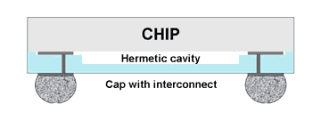 FIGURE 1: Cookson Electronics’ interconnect on cap.
 |
Some companies, like Shellcase, have succeeded in making inorganic packages that may be silicon or a combination of silicon and glass. This Israel-based company has developed WLCSPs (wafer-level chip-scale packages) for MEMS and optical chips (glass cap). Packages are constructed primarily of inorganic materials; some organic adhesive is used, however. Shellcase singulates chips with a “V” cut to form edges with external metal conductors that extend onto a second glass layer on the opposite side where solder bumps can be formed. The chip is sandwiched in glass when optical chips are used. Figure 2 shows the construction.
 FIGURE 2: Shellcase’s interconnect on chip.
 |
Time, and further developments, will determine how the silicon package will fair, and whether the best connection scheme is through or on the chip, or by means of the cap. But one issue remains, and it is the same as for flip chip: The low coefficient of thermal expansion of the silicon structure will be mismatched to that of a substrate that is generally an organic material.
Dr. Ken Gilleo is with ET-Trends LLC; et-trends@cox.net.


Press Releases
- Changes in Incap’s Management Team: Incap updates its leadership model to support its growth strategy
- Niche Electronics Celebrates Completion of Florida Expansion
- Microscreen Names Nik Thomas Director, Expands Leadership Role Amid Continued Organizational Growth
- W&S Enters New Growth Phase Through Strategic Partnership and New Leadership