

2005 Articles
Maximizing Mixed-Technology Applications
How pin-in-paste cuts wave soldering time and costs.
Manufacturers are faced with the competitive challenges of reduced labor costs, faster time-to-market and the need to fully utilize existing manufacturing resources. While there are countless examples of how this can be accomplished, one front-of-the-line process can be used to greatly diminish end-of-the-line costs: pin-in-paste technology. This novel approach to through-hole component placement can result in dramatic cost and time savings.
While it has become increasingly common to have assemblies that are completely SMT, in many situations one or two components – usually connectors – need to be inserted and then wave- or hand-soldered. Valuable time and costs can be eliminated by printing solder paste into the through-holes at the same time that SMT printing is occurring, placing the surface-mount and through-hole components and then reflowing these components simultaneously.
In many cases, adequate amounts of solder paste cannot be deposited into the plated through-holes with the conventional squeegee method of screen printing. Therefore, alternative techniques must be used to meet the paste volume requirements for thick boards. One such alternative is the use of enclosed print head technology to ensure proper hole filling. Rather than trapping paste between squeegee and stencil, as is the case with traditional printing, the enclosed print head uses direct pressure to force paste into stencil apertures and board holes. Studies have shown that this method delivers better PTH paste penetration than is obtained with squeegees.1
In general, paste usually penetrates further through larger diameter holes than through smaller ones, and balancing a wide range of diameters on one board can sometimes be difficult. But with only one or two connectors on each board, this rarely occurs. There are a couple of solutions, though, if this problem does arise. One technique is to restrict the flow of paste into the larger holes by leaving a bar across the stencil apertures. The other method is to use special board support whereby small pillars can be positioned under the larger holds to plug them.
Component placement is straightforward and best results are achieved when the component leads are cropped reasonably short – not more than 1 to 1.5 mm longer than the board thickness. If all components are autoplaced and inserted, the order of assembly will depend on how the line is configured. If the leaded devices are hand-inserted, it is usually better to do this after the surface-mount devices have been placed to prevent heavier, leaded devices from being damaged by the shaking of the placement machine or its heads crashing into these taller components.
Some special reflow considerations exist when employing pin-in-paste technology. Since 50% of the volume of the paste is flux, the ramp to liquidus needs to be slow so that boiling flux does not eject paste from the holes. If the solder joints are held above liquidus for several seconds, the probability of voids is dramatically reduced. Finally, it may be necessary to re-educate inspectors to recognize good wetting, as the fillets will have a somewhat different appearance than those that have been wave soldered (Figure 1).
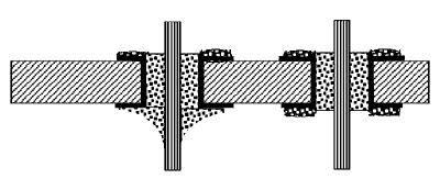 FIGURE 1: Classic wave soldered joint (left), and printed through-hole joint (right).
 |
To conclude, I will leave you with a real-world example of the advantages of this process. One of our multinational customers saved four minutes per board in connector assembly time (one minute with pin-in-paste versus five minutes with wave) and also reduced the number of operators needed to hand insert components by 35 (25 operators with pin-in-paste versus 60 with wave). That is what I call a major productivity improvement!
References
- D. Manessis, M. Whitmore, J.H. Adriance and G.R. Wesby, “A Characterization Study of Direct Imaging Technique for Stencil Printing of Thick boards (0.125") in the Alternative Assembly and Reflow Technology (AART) or Pin-in-Paste Process,” IEMT - Board Level Assembly, Semicon Southwest, 1998.
Clive Ashmore is global applied process engineering manager at DEK (dek.com). His column appears semimonthly.


