

2005 Articles
Front-End and Back-End Boundary Blurs
SemiCon West shows an increasing number of devices packaged at the wafer level.
More than 40,000 people gathered in San Francisco at SemiCon West in July. Why so many? This year, SEMI combined the front-end and back-end shows. Combining the show was partly a matter of convenience for exhibitors, but it is also symptomatic of trends in semiconductor manufacturing. Historically, the semiconductor process ended with the completion of wafer fabrication. The next steps in the IC process focused on what was known as back-end assembly or IC packaging. Today the distinction is not so clear. A new dynamic is underway as front-end wafer processing and back-end assembly converge and the pace accelerates rapidly. After the wafer is fabricated the die may no longer be “packaged” in formats with which industry has long been familiar. Processing at the wafer level now includes redistribution and solder bumping, gold bumping, wafer level packaging and post-passivation layer processing such as the addition of thick copper.
The International Electronics Manufacturing Technology symposium held during SemiCon West focused on manufacturing at the wafer level. An increasing number of devices are packaged at the wafer level including analog devices such as power amplifiers, battery management devices, controllers, memory and integrated passives. Most of these devices are relatively small in size, and thousands can be fabricated on a single wafer.1 Presentations on WLP included an overview of business issues related to wafer bumping at ASE and the use of wafer-level applied underfill materials (“Microfil”) described by National Semiconductor. Both ASE and National highlighted trends in increasing pin counts for WLPs and bumped die.
Not only has manufacturing moved closer, but the need for communication between people in the various segments of semiconductor fab and assembly has become critical. The challenges in assembly with the introduction of copper low-k silicon were described by LSI Logic during the IEMT symposium. Challenges include assembly material selection such as the underfill material, method of wafer dicing, wire bond characterization and mold compound selection, and issues with the movement to Pb-free bumps on the die. LSI Logic highlighted the importance of co-development and partnerships for this new era.
Driven by the need for greater functionality in smaller spaces, speakers from Intel, Qualcomm and startup SyChip described various forms of system-in-package (SiP) in production. Intel noted the difference between the MCP era and the drivers for the SiP. Highlighted was the value proposition that the integration of highly valued elements into a smaller form factor delivers new end-user capabilities sooner at a lower cost. Qualcomm described its new stacked module package (also called package-in-package) and its development drivers. SyChip described the fabrication process for its SiP solution called a chip scale module. The modules feature flip-chip die mounted on the thin-film on silicon substrate containing integrated passives. The plug-and-play solution provides RF capability in a tiny package. Henkel Technologies provided details of the testing and qualification of material sets for SiP.
Regardless of the package format, bare die testing is a critical issue. Micron described DRAM/PSRAM bare die testing, emphasizing the expense of bare testing at the wafer level given test time requirements and other factors. Also highlighted were the equipment limitations, power supply requirements, temperature requirements and the correlation of the package in terms of quality and reliability.
WLPs, solder and gold bumping are considered post-passivation layer (PPL) processing, but several additional applications are also emerging. PPL in a broader view includes the addition of thick copper for power distribution, a stress buffer layer, multilayers for redistribution or on-chip integrated passives.
During the Advanced Packaging and Interconnect Alliance (APiA) symposium, Megic described its post-passivation technology (Figure 1). Megic considers its process to be an application of circuit board processing technology to IC wafers. Called “Freeway,” it provides two metal systems: copper interconnects for flip-chip applications, and gold interconnects for wire bonding and TAB applications. The architecture uses PPLs for global interconnections, and IC fine-line metals under the passivation layer for local interconnections. The architecture is similar to that of traffic networks for cars, buses and trucks. For the copper interconnect, Megic’s process is provided in Table 1.
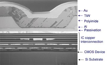 FIGURE 1: Cross-section of Megic post-passivation interconnection: 4 µm thick gold over 5 µm polyimide and encapsulated with 5 µm polyimide (not shown). The post-passivation interconnection is built over a 0.13 µm CMOS embedded microprocessor with 8 layers of damascene copper under the passivation layer.
 |
Inductors can be formed with Megic’s process using thick metal (>3 µm gold or copper) and thick dielectric (>3 µm polyimide). The inductors provide >20 quality factor that outperforms the inductors formed by the IC process under the passivation layer (Q<10). The two-layer copper post-passivation metals reduced the ground surge of a 1 GHz, 8Mbit SRAM from 270 mV to 130 mV. One layer of gold post-passivation metal reduced the voltage supply from 1.5V to 1.2V for a 1 Gbit network chip.2 PPL processing is in production at a variety of companies including Freescale Semiconductor, STMicroelectronics and Texas Instruments.
APiA also focused on packaging challenges ranging from high-value, low-volume devices such as FPGAs to high-volume memory products with speakers from Altera and TechSearch, respectively. Thermal issues with high performance microprocessors as viewed by AMD and new resists material developments from AZ Electronic Materials were also discussed. Freescale provided case studies of the development of SiP for mobile communications.
There is no shortage of new package developments ranging from SiP solutions to increased integration and processing on the wafer. As the infrastructure continues to develop and the cost of packaging at the wafer level declines, the use of the technology will expand into higher volumes and a greater number of applications. The front- and back-end processes will converge, offering increased sales of equipment and materials. The future for WLP is bright.
References
- E. Jan Vardaman, “Expansion of Wafer Level Wafer Packaging,” ICEP Proceedings, Tokyo, April 2005.
- M.S. Lin, et al, “A New System-on-a-Chip (SOC) Technology – High Q Post Passivation Inductors,” IEEE 53rd ECTC Proceedings, May 2003.
E. Jan Vardaman is president of TechSearch International, Austin, TX; jan@TechSearchInc.com. Her column appears semimonthly.


Press Releases
- XLR8 EMS Welcomes Raul Jorge Lopez Jr. as Director of Program Management and Procurement
- Koh Young America Promotes Ramiro Mora to Lead Service and Applications in Mexico and South America
- ViTrox Americas Welcomes Huy Pham as Technical Support Engineer
- XLR8 EMS Appoints Steve Dutton as Chief Sales Officer