

Current Issue
Manufacturing Test Solutions for SSDs
A new system performs both ICT and boundary scan in high-volume settings.
A solid state drive or disk is a data storage device that functions like the traditional hard disk drives and is used on tablet PCs, laptops, servers and network storage for cloud computing.
The SSD has no moving mechanical parts. Instead, it makes use of NAND flash devices to store data. SSDs are the preferred storage where space and battery life pose constraints, commonly tablets and notebook PCs. SSDs are also used in server and network storage, mainly due to their reliability, durability and speed.
Sizes and types of SSDs can be classified according to their market applications:
- Enterprise SSD: Targets network server as well as companies that provide and maintain cloud computing applications.
- SSD HDD: Targets laptop and desktop PC as direct replacement for traditional hard disks.
- Tablets/notebook PC SSD: The smallest type of SSD; targets tablet and smaller/slimmer notebooks.
Just like any memory storage device, SSD reliability and quality is very important, as it holds important functions, whether for consumer or commercial applications. Any hardware failure means data loss for the end-user, or even more catastrophic consequences if used in commercial applications. To ensure that SSDs have the required quality level, they are subject to a series of tests in the manufacturing process before the devices are shipped to the end-user or integrated into devices such as servers, laptops, tablets and other devices.
The first important test in the manufacturing process is structural test. This ensures that components are correctly placed and that there are no manufacturing failures, such as solder shorts and open pins on components.
Enterprise and hard disk drive SSD. Both enterprise SSD and the HDD SSD models can use in-circuit test (ICT) since the PCB real estate still permits placement of testpoints. In-circuit testers are the most commonly deployed test systems used to capture structural failure during manufacturing. Here are typical tests that will be performed during ICT:
- Shorts and opens testing: Unpowered testing of solder shorts or opens.
- Analog device testing: Unpowered testing of resistors, capacitors, inductors, and transistors.
- Digital powered test: Powered testing of digital devices.
- Analog powered test: Powered testing of voltage regulators.
- Boundary scan-powered shorts test: Testing for shorts between boundary scan pins and nearby non-boundary scan pins with testpoints.
- Boundary scan interconnect and buswire test: Boundary scan test for interconnect pins between boundary scan devices.
- Boundary scan connect test: Boundary scan test for pins not connected to any device and that have testpoints.
- Silicon Nail: Novel interconnect test between boundary scan device and non-boundary scan device.
- Cover-Extend: Novel interconnect test between boundary scan devices and non-boundary scan device using vectorless technology.
Integration of benchtop boundary scan tools can also help to increase test coverage and throughput with the following tests:
- Boundary scan interconnect and buswire test.
- Boundary scan pull-up/pull-down resistor: Testing of pull-up/pull-down resistors connected to boundary scan pins.
- Autobank for NAND Flash or DDR devices: Parallel testing of NAND flash or DDR devices.
- Cover-Extend.
Full ICT test is normally not implemented until the high-volume manufacturing test stage. In the initial prototype and new product introduction (NPI) phases, using a benchtop boundary scan tool offers some advantages:
- Manufacturing test is enabled and fine-tuning can be performed at the earliest possible stage of product development.
- Significant cost savings on development and debug of the boundary scan test for volume manufacturing test, as the test developed on PC boundary scan tool can be executed at the ICT manufacturing test stage, if integrated into ICT.
- Integration of PC boundary scan tool in ICT during volume manufacturing will shorten development time, hence improving time-to-market.
Not all SSDs are testable using ICT. Due to consumer demands for smaller, faster and longer battery life devices, the size of every component in electronics devices is also shrinking, including the printed circuit board.
Tablet/Notebook SSD. The smallest SSD form factor currently available in the market is the M.2 SSD (Figure 1), which supports the mSATA and PCIe interfaces normally used on tablet and notebook PCs due to their size and speed. Figure 2 shows the block diagram of an M.2 SSD, which consists of the NAND controller and NAND flash device.The key manufacturing test challenges faced by tablet/notebook SSDs and smaller-sized HDD SSDs are that testpoints are limited, and very often these are available only for some critical nodes such as power and boundary scan pins. For this type of SSD, the boundary scan tool system is the only solution possible for manufacturing test.
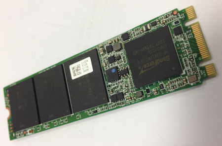
Figure 1. M.2 SSD for tablet and laptop PC, the smallest commercial version.
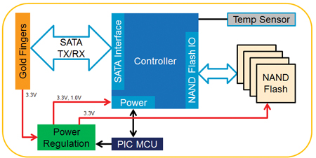
Figure 2. Typical tablet PC SSD block diagram.
PC Boundary Scan Test. PC boundary scan test can involve the following:
- Boundary scan interconnect and buswire test. Although there is only one boundary scan device, the interconnect and buswire will still be able to test a few pins that are interconnect or pins that have a self-monitoring boundary scan cell.
- Boundary scan pull-up/pull-down resistor.
- Boundary scan silicon nail: Tests interconnection between NAND controller and NAND flash devices.
- Loopback test between SATA/PCIe and NAND flash controller.
- Cover-Extend test for non-boundary scan devices and connectors.
In some cases programming is needed for SEEPROM, SPI flash and PIC devices.
There are limitations with using only the benchtop boundary scan tool, though. One is the issue of not being able to perform unpowered and powered tests, as an ICT system can. To resolve these limitations, a dedicated SSD manufacturing test solution has been developed to perform both ICT and boundary scan test during volume manufacturing testing.
Setup of the manufacturing test system for SSD. The manufacturing test solution for SSDs comprises a benchtop boundary scan tool, measurement instrumentation and programmable power supply, with both hardware and software integrated. This solution is capable of performing unpowered short and open test using resistance measurement, as well as voltage measurement. This will ensure that important power nodes are tested the same way as they are in ICT. An advantage is that this is a lower-cost system compared with conventional ICT.
Advantages offered by the various instruments in this system include:
- Unpowered resistance measurement before powering up.
- During power up of the SSD PCBA, voltage and frequency measurements ensure that all the voltage rail and frequency on board are correct.
- Multiplex power supply, measurement and boundary scan test on a panel board.
The programmable power supply offers these benefits:
- Ability to control the supply voltage for the SSD board.
- Single universal power supply for different types of board and voltage requirements will enable testing of multiple SSD types.
The SSD manufacturing test solution will need a fixture (Figure 3) that will enable testing of a panel of SSD PCBAs for throughput enhancement and ease of handling by the production operator.
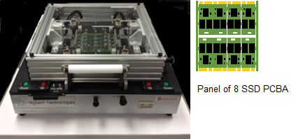
Figure 3. SSD fixture testing a panel of 8 SSD boards.
Such an SSD manufacturing test solution provides the following test coverage (Figure 4):
- NAND controller, including loopback to SATA/PCIe interface.
- NAND flash.
- DDR memory.
- PIC device.
- Resistance and voltage measurements on voltage rails.
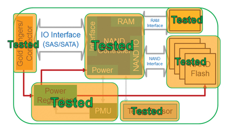 Figure 4. Test coverage offered by SSD manufacturing test solution.
SSD manufacturing test software. Software for test development in this test solution automatically integrates the following capabilities:
- Generation of the boundary scan test using board CAD data, BSDL and non-boundary scan test libraries.
- Setting the programmable power supply voltage and controlling the power on and off.
- Generation of measurement system commands to measure resistance, voltage and frequency on board.
- Generation of fixture wiring information for the fixture vendor.
- Generation of the manufacturing test sequence (Figure 5), which includes data logging of board serial number, pass/fail information and failure details (Figure 6).
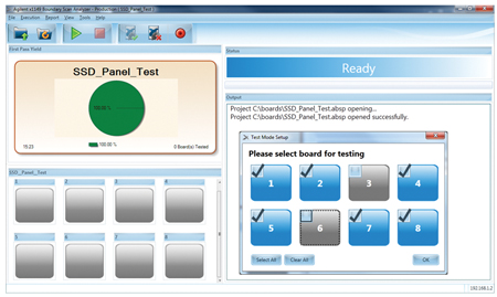
Figure 5. Production SSD test interface.
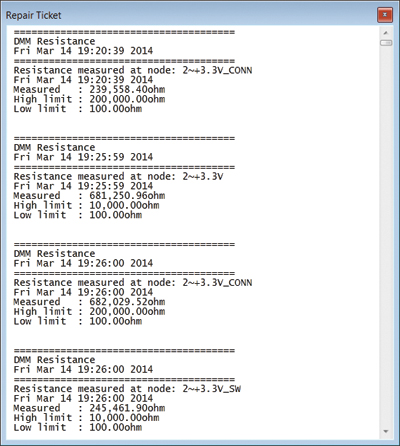
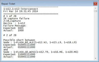
Figure 6. Failure ticket showing easy-to-read failure messages for operators.
This new solution permits testing of SSDs with smaller form factors during volume manufacturing. By integrating available measurement and testing tools supported with the development and production software interfaces, quality SSD boards can be ensured.
Jun Balangue is a technical marketing engineer at Agilent Technologies (agilent.com); jun_balangue@agilent.com.


