

Recent Advances in PCB Manufacturing Equipment

More lasers and improved and integrated software have factories humming.
The methods and equipment used to fabricate PCBs are becoming increasingly advanced and centralized. For example, computers, lasers, and AI are ever more common in all areas of PCB processing. In recent years, a considerable number of PCB manufacturers have invested heavily in the integration of the complete shop, with all equipment controlled by one central computer. The interconnection enables quicker file processing, higher accuracy, and improved yields.
One of the most expensive pieces of production equipment is the laser-direct imaging system (LDI), which has made significant improvements in accuracy, speed, quality, and in reducing overall manufacturing rejects. The newer models feature multiple cameras to locate lamination holes, compare them to the original Gerber file, then digitally scale the image to fit the panel. Newer laser imagers are capable of imaging down to 15µm line widths and spaces.
CAD/CAM software (computer-aided design and computer-aided manufacturing) is used to design and manufacture prototypes, finished products, and production runs. An integrated CAD/CAM system offers a single complete solution for design through manufacturing. From the beginning of a new PCB order, CAM software is used to inspect Gerber files, perform a design rule check, and identify trace or hole violations that could result in shorts or opens later in the process. The software checks impedance throughout the circuit traces and layers. It adjusts for laminate shrinkage by calculating scaling and resizing each layer to compensate. The software calculates etchback on traces and optimizes the job for maximum yield.
The software then coordinates feedback from post-lamination alignment and x-ray drilling and adjusts each layer’s scaling in a database to ensure tight layer-to-layer alignment. The software then sends all the relevant information to the drills, routers, testers, imaging equipment and any other machines connected to the company’s own intranet.
One major change has been the addition of laser technology to many operations and machines, from laser drills that sculpt through laminate, to lasers that cut to specific programmable depths to create blind microvias. Excise lasers built into automatic optical inspection (AOI) units can easily remove small shorts, and new technology even permits 3-D printing of copper to repair opens in the circuit, greatly improving yields.
Computer controls enable higher accuracy in the alignment of innerlayers by detecting errors in scaling with x-ray imaging and then correcting the drill files to correctly align tooling holes for lamination and drilling.
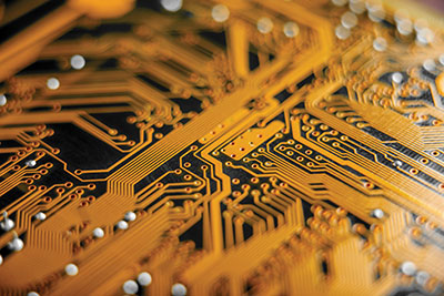
Figure 1. Advancements across a range of fabrication processes have boosted yields.
As such, today’s drills are much superior to the machines of only a few years ago. They now offer laser drill size detection, broken bit detection, and feature drill canisters that automatically change bits due to wear or hit counts. These drills feature controlled-depth drilling for backdrilling of vias to reduce capacitance and improve impedance. Newer drills feature very high-speed drilling – up to 250,000rpm – with air-bearing heads and very accurate table servos. In addition to typical mechanical drilling, manufacturers use laser drills, powerful UV lasers that cut through copper and laminate to form microvias one or two layers down; thicker copper stop pads are used to halt the laser. Laser drilling is essential for HDI or very fine-featured PCBs.
To improve innerlayer drill registration, as mentioned earlier, x-rays look inside the PCB for special alignment pads that may have been compromised and then find the best location for the pads. The software subsequently calculates for stretch or shrinkage in the panel’s size after lamination, and automatically adjusts the drill file size by using scaling and drill alignment holes so the drill will more accurately find the center for all pads. The machine will communicate with the drill, giving it new x-y and offset stretch coordinates to increase or decrease the data file position and size of the panel for greater accuracy.
Inkjet solder mask labeling units have replaced the outdated, messy and inaccurate silkscreen method. The machine has multipleinkjet heads that quickly spray accurate lines, letters and drawings in white ink on the finished solder mask. A powerful UV lamp dries and cures the ink as it is applied to the PCB. This eliminates the mess and issues associated with silkscreen application; e.g., the flip table, squeegee, etc.
Computers now control plating bath chemistry through constant monitoring and titrations. They may sense a deficiency in one of the many chemicals, for example, and automatically add the right amount of specific chemicals to correct the bath. Measuring and adjusting are performed in real time. Chemical baths do not suddenly go out of spec; therefore, important parameters such as copper ductility remain well-controlled.
Inkjet solder mask units have two different methodologies. Older ones spray the entire board, which is then imaged with an LDI and developed, then cured. Newer inkjet solder mask units apply the mask ink directly on the board, with openings for vias. A powerful UV light then cures the solder mask.
Lab computers enable quicker cross-sections and easier spotting of potential problems before boards are shipped. Computerized tracking using barcodes and/or QR codes show in real-time which jobs are behind schedule.
Newer flying probe electrical testing is much faster than the old systems, and is especially cost-effective for high-mix, low-volume production. The improved speed and accuracy eliminate the need for older fixed-bed ICT custom fixture-based testing, which is expensive, not cost-effective for short product runs, and requires much longer lead times to create the custom fixtures.
Laser-cutting quickly and very accurately shapes and cuts flex circuits, eliminating the old kick press and steel rule die method.
All fabricators seek to reduce costs, but a PCB fabricator lives or dies on its yields. A single LDI can cost well over a million dollars, but the payoff can be tremendous. In the past, a 70% yield was a sign that a fab shop was doing well. Today, with increased automation in manufacturing, shop yields are 90% and up.
is chief executive officer of Rush PCB Inc., a printed circuit design, fabrication and assembly company (rushpcb.com); roy@rushpcb.com.


