Defining Acceptable Voiding Levels Under QFNs
 Will IPC accept the >50% voiding recommendation?
We have long had numerical guidelines for voiding levels below which we deem acceptable for BGA joints. Originally from IPC documentation, the limit called for less than 25% voiding of the joint area when the joint is looked at from the top-down in x-ray. More recently, and entirely because of evidential data, this has been increased to 30%.
Many other joint types also given designated qualifications in the IPC guidelines, such as through-hole joint fill levels, can be evaluated using x-ray. However, there has always been an anomaly in the level of voiding in bottom termination components (BTCs). To date, no evidence-backed, indicative values are published detailing acceptable voiding in these joints and, in particular, the large central pad under QFNs.
The primary reason for this is the lack of appropriate data upon which to base a criterion. Without evidence, the standards writers cannot propose values that will impact how our industry does business. For QFNs, however, this is now all set to change. For that we thank Dave Hillman, chairman of the IPC Voiding Task Group, and his merry band of volunteers. I had the good fortune to listen to Hillman’s presentation at the recent SMTA International Conference for Electronics Enabling Technologies (ICEET) titled “Reliability and Voids in QFN Solder Joints: What’s the Issue?” Hillman showed data from device manufacturers that indicate thermal performance of large central MLF pads as a function of solder void. (See IPC-7093, Figure 6-19.) This is a performance criterion, however, and while it may set an upper voiding limit to define a failure level, it does not necessarily indicate what value(s) could, or should, be used as a manufacturing process indicator. To correct for this, Hillman presented initial data on lifetime solder joint integrity as a function of void size in QFN central pads for tin-lead and lead-free solders. Further papers on this topic will be presented this month at the SMTA International Conference.
From these data, Hillman and his team are recommending modifying IPC J-STD-001, section 7.5.15, Bottom Termination Components (BTCs), to indicate that, under manufacturing best practices, voiding in the central pad termination be less than 50% of the available wettable area. This recommendation has yet to be voted on by the appropriate IPC committees. Therefore, as Hillman says, those who have any comments or concerns as to why this should not be the case, especially backed with data, should make their representation to the task group, which meets at the next IPC Apex Expo conference in February.
Note that this guidance is only for the large central termination under QFNs. It does not give a suggested value for maximum voiding under the typically smaller QFN edge terminations. The task group does not have data for this. Therefore, for edge terminations, acceptable voiding levels still need to rely on contracted rules between assembler and customer. (Unless, of course, you have good data that can be shared with the task group to help define this as well!)
The other point to note is the term “available wettable area.” This is because QFNs in the dataset used did not have vias in the central pad. When vias are present, they can be seen as low-density areas in the x-ray image and included in the calculation as “apparent void areas” by typical x-ray system void calculation software. These “via voids” should not be included in the total void calculation when determining whether a process is within its parameters. Finally, this recommendation is a limit for the total voiding level. There is no clause for the maximum size of a single largest void within the total area, something I have observed has often been discussed in setting void limits under QFNs. Again, this cannot be designated in the committee’s recommendation at this time owing to lack of hard evidence.
As examples of the proposed recommendation, consider the following images:
FIGURE 1 shows two QFNs with differing levels of voiding under the central termination. In neither device are vias located over the central pad.
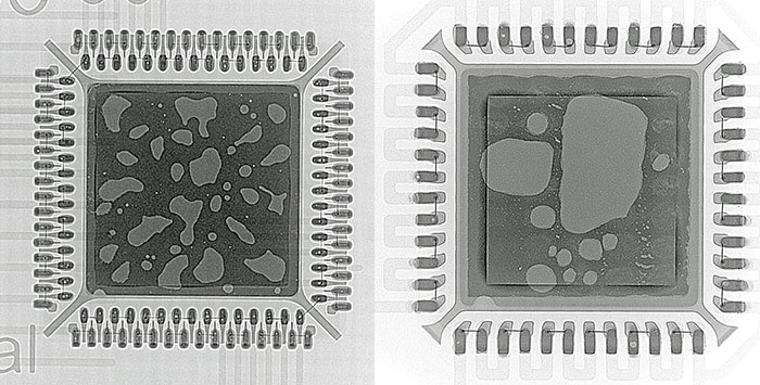
Figure 1. Two QFNs with different levels of voiding under the central termination.
FIGURE 2 shows the void calculation made by the x-ray system on the two QFNs in Figure 1. The calculations indicate the QFN on the left has total voiding under the central pad of ~30%. The QFN on the right has just over 50% voiding under the central pad, thereby exceeding the proposed guidelines.
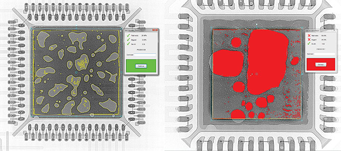
Figure 2. Void calculations.
FIGURE 3 shows an x-ray image of a QFN with vias located over the top of the central pad. Note the vias on the left are much lighter in grayscale compared to their surroundings. In this sample, some vias also include some solder in their depth, making them much darker than their surroundings. Both situations will impact the typical x-ray system void calculation when undertaken on this type of image (see Figure 4).
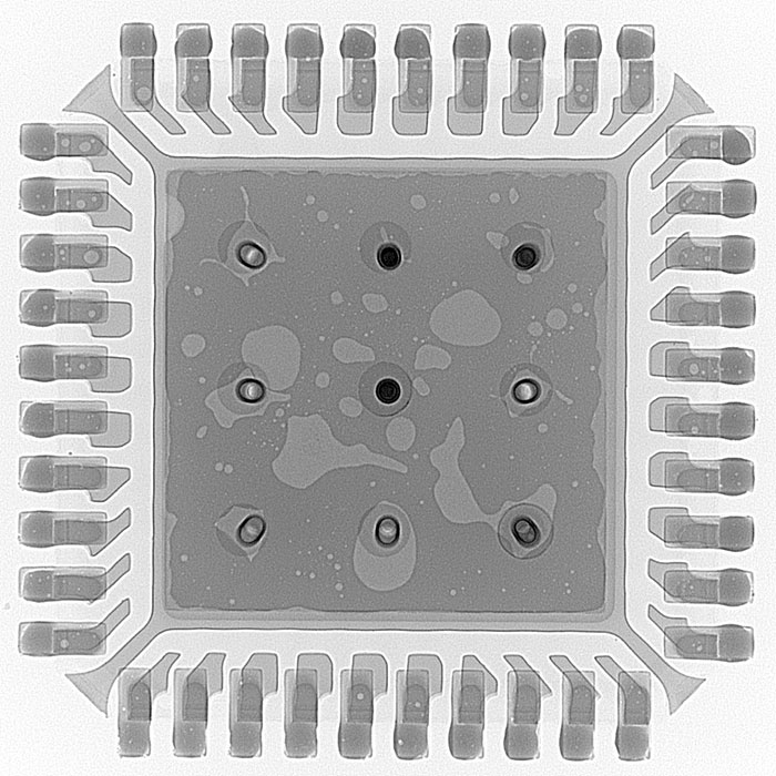
Figure 3. X-ray image of a QFN with vias located over the top of the central pad. Vias on the left are much lighter in grayscale due to the presence of solder.
Figure 4 shows the software void calculation both without (left) and with (right) adjustment/allowance for the vias of the device in Figure 3. Without adjustments (left), the void calculation is ~21%. By excluding areas around each via using additional software features (blue boxes, as seen on right) the void calculation becomes ~16%. Both are within the proposed guidelines but also indicate differences will occur and will be especially meaningful if “voids” from the vias push the total voiding above the suggested level.
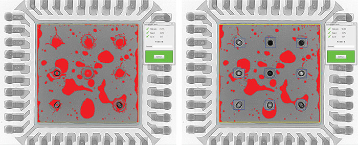
Figure 4. Software void calculation without (left) and with (right) adjustment/allowance for the vias of the device in Figure 3.
An alternative approach to editing regions from the x-ray image before making the voiding calculation is to take a schematic of the device and compute the total area percentage covered by all the vias as a function of the total pad area. This value can then be subtracted from the software calculation made from the original x-ray image and without making any additional modifications. However, will you remember the correct value to subtract for each QFN in each board? And what if there is “real” voiding at the pad location under specific vias? In this latter situation, the voiding will not be included in the calculation.
Another more interesting approach is to use the PCT technique, if available on the x-ray system, to make a 3-D model of the QFN and select only the pad slice level and make the software calculation only at that depth, thereby removing the vias from view completely (and also from any calculation).
FIGURE 5 shows 3-D representations of the PCT model created for the device in Figure 3. The position of the vias above the central pad is clear and indicates the location of the solder down some of the vias.
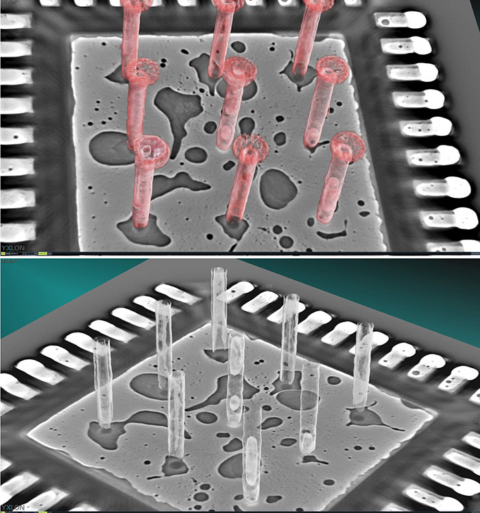
Figure 5. 3-D representations of the PCT model created for the device in Figure 3.
FIGURE 6 shows 3-D representations from the PCT model only at the pad level in the device. All other information has been removed. Using these data permits the software void calculation to be made on the reconstructed 2-D slice at this level only, as seen in Figure 7.
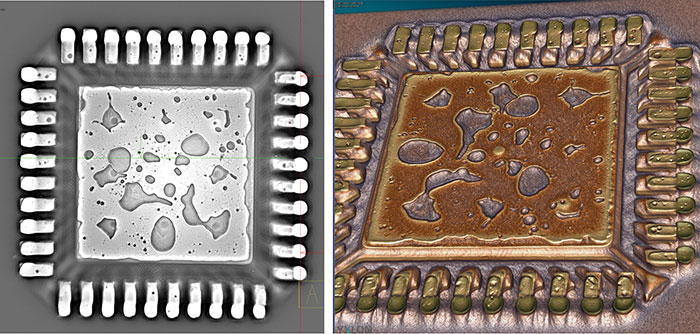
Figure 6. 3-D representations from the PCT model at the pad level in the device.
FIGURE 7 shows the reconstructed 2-D slice at the pad level in the QFN shown in Figure 3 and the software calculation of the total voiding at this level, which is ~24%, again well within the proposed guidelines.
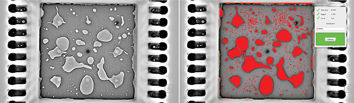
Figure 7. The reconstructed 2-D slice at the pad level in the QFN shown in Figure 3.
It is worth noting, for most x-ray systems, additional error in the voiding calculations can be caused by how the pad area is defined for the computation. This could be manually, such as by drawing a rectangle around the pad, or by setting a grayscale threshold and letting the software define the pad limits. Whichever approach is used, it is possible to make the value of the pad area smaller or larger than its true number. This will have a meaningful impact on the total void calculation, as the total void area seen in the image may be divided by a smaller or larger value for the pad area than it should be. Therefore, I would suggest all these voiding calculations be considered to include a reasonable error bar of a few percentage points; adjust internal process indicators accordingly. Do not consider voiding of 49.9% = good and 50.1% = bad. Apart from the likely error in the measurements, this misses the point of a process indicator: if voiding is in the ~40-50% range, should this not make you ask questions of your process?
Subject to agreement and approval, for the first time there will be a guideline for the acceptable level of voiding present under central pad terminations of QFNs. It says manufacturing best practices is voiding less than 50% of the available wettable area. Many x-ray systems can make these calculations, but consideration must be given as to the nature and structure of the device so that vias seen as voids, for example, are not included in the calculation. •
Au.: Images courtesy Peter Koch, Yxlon International.
, is an expert in use and analysis of 2-D and 3-D (CT) x-ray inspection techniques for electronics; dbc@bernard.abel.co.uk.


