Unreflowed Solder Under QFNs
 Is the reflow profile the problem? X-ray can help.
Looking through some recent x-ray images of what I would call “good bad” boards (at least, that is what they are for me, as they showcase “good” examples of how certain “bad” types of failure look under x-ray inspection), I came across a number of different issues that are different from “traditional” BGA/QFN problems mentioned in this space before. To wit, I noted some images showed where solder paste had not reflowed under the devices, and there was the presence of foreign object(s), such as discrete components, trapped under the package.
FIGURES 1 and 2 show how unreflowed solder paste typically looks under QFN joints in an x-ray image. In the magnified view (Figure 2), individual grains of the solder paste are seen clearly, instead of appearing as a typical single smooth continuous joint. The cause of this is probably not an insufficient reflow profile. Rather, it is more likely the board has not been reflowed at all. As it may be desired, or necessary, to x-ray inspect (representative) boards after placement but before reflow as part of a quality control process, it is worth noting this characteristic shape of the solder under the components is different from what would be expected post-reflow.
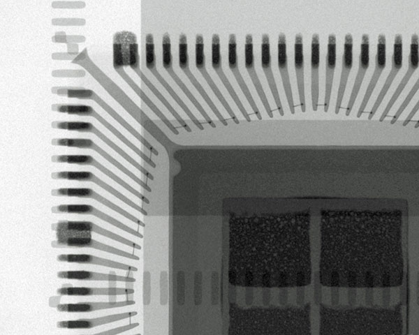
Figure 1. Top-down x-ray image of QFN with unreflowed solder joints.
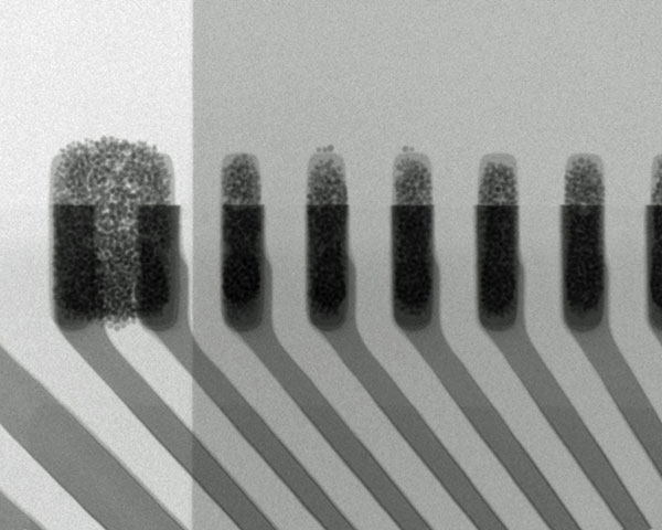
Figure 2. Top-down magnified x-ray image of QFN with unreflowed solder joints.
A similar situation can be seen in the following x-ray images for unreflowed solder paste under a BGA. FIGURE 3 is a top-down view, and FIGURES 4 and 5 are oblique-angled views. In the top-down view (Figure 3), individual solder grains can be seen surrounding the base of some of the solder balls. However, oblique angle views show more clearly that no reflow has taken place across all the joints. As ever, just looking from the top-down in an x-ray inspection may not show all the issues. Oblique angle views are often needed to complete/confirm the situation. These images indicate the typical view of a BGA post-placement and prior to reflow. During reflow, the solder grains coalesce and merge with the BGA solder ball.
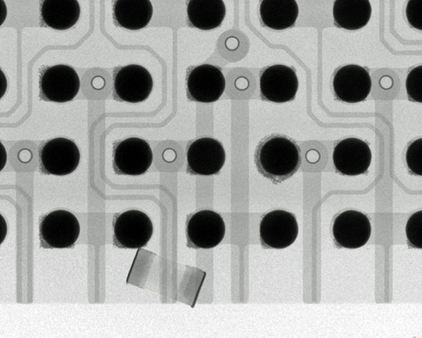
Figure 3. Top-down x-ray image of BGA with unreflowed solder joints and a foreign object underneath.

Figure 4. Oblique view x-ray image of BGA in Figure 3.
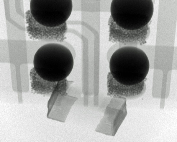
Figure 5. Magnified oblique view x-ray image of BGA in Figure 3.
Figures 3 to 5 also show a discrete component trapped under the BGA. Under x-ray inspection, such a foreign object is clearly visible, but would not be seen optically in this example unless all sides of the component were patiently examined using a side-viewing microscope. If the rogue object were farther toward the center of the BGA, then even that type of optical inspection would likely miss it. While the risk of this type of issue is the component could solder to and/or short adjacent connections, it may be it has no apparent interaction at all, as in this case, and could be entirely benign in terms of circuit operation. Although, the height of the component could lift the BGA away from the board and therefore cause issues for a greater number of other BGA solder balls by preventing their contact with the paste at reflow. This could cause the opportunity for open joint(s) or head-on-pillow failure(s) to occur. My other question is where has this device come from? Is this component missing from where it should be, or has there been extra component(s) left for some other equipment operation reason?
Unreflowed solder paste has a very different characteristic look in x-ray images compared to its reflowed state. The usefulness of pre-reflow x-ray inspection on boards is not compromised by the operator seeing something very different from what would be normally expected during the typical manufacturing quality process. Such a characteristic presentation will also help confirm if there is an issue for post-reflow fault-finding.
Seeing unwanted foreign objects under components will allow remedial action such that, even if they do not appear to be causing an obvious and direct problem, their opportunity for doing so in the future can be removed before product reaches the field.
, is an expert in use and analysis of 2-D and 3-D (CT) x-ray inspection techniques for electronics; dbc@bernard.abel.co.uk.


