Heterogeneous Integration a Recurring Theme at ECTC
 TSV has become reality. How many ways can it be used in 3-D packaging?
The IEEE Electronics Components and Technology Conference (ECTC) welcomed more than 1,500 attendees to Las Vegas. Registrants in the hallways pondered the impact of trade disputes, while conference sessions focused on the latest developments in electronics packaging. A preconference workshop provided insight into progress on the Heterogeneous Integration Roadmap activity. (Per IEEE, heterogeneous integration is the integration of separately manufactured components into a higher-level assembly such as SiP that, in total, provides enhanced functionality and improved operating characteristics.) Several chapters are almost ready for release. Throughout the conference many presentations focused on heterogeneous integration packaging solutions. A number of companies have proposed a strategy of chiplets to achieve the economics of scaling previously achieved with silicon scaling. A variety of new architectures were described at ECTC.
A New 3-D Era
The industry is moving into a new era of 3-D integration with many formats. Adoption of through silicon vias (TSVs) has become reality. The hallway discussion is no longer about when TSV will happen, but rather on the multitude of ways TSVs enable the required packaging solution. Of course, a TSV solution is not appropriate for every 3-D application, but the industry is seeing increased adoption of the technology.
GlobalFoundries and ASE discussed a die-to-wafer (D2W) process for 3-D packaging of logic on advanced semiconductor nodes. CEA Leti and STMicroelectronics detailed research on a new 3-D architecture using chiplets on an active interposer. TSMC presented its system on integrated chips (SoIC) process for 3-D heterogeneous integration, in which an active wafer is used instead of a passive interposer. IME A*Star described an active TSV interposer-based IC design, fabrication, assembly and test process. Researchers from UCLA discussed through wafer via development for a silicon interconnect fabric and presented work with Keysight Technologies in the integration and characterization of indium phosphide (InP) on the silicon interconnect fabric.
New developments in high-density packaging were discussed as alternatives to silicon interposers. TSMC discussed its high-density large package using a six-layer redistribution layer (RDL) interposer to connect four silicon chiplets and two HBMs.
Many organizations discussed developments in materials, equipment and processes to permit wafer-to-wafer (W2W) and D2W bonding. While many presentations focused on Cu-Cu bonding, EV Group described recent work on Al-Al direct bonding. Organizations such as CEA-Leti, Fraunhofer IZM-ASSID, IME A*Star, IMEC, Sandia, Xperia and many universities continue work on processes. While examples of hybrid bonding at image sensor companies including Samsung, Sony and STMicrolectronics are well known, companies including TSMC have this technology on their high-performance technology roadmaps. Samsung described some of its latest work on Cu-Cu hybrid bonding, focusing on grain size and orientation to improve connection and reliability.
Many versions of package-on-package (PoP) were presented this year. TSMC packed the room with a paper on its 3-D Must-in-Must technology for advanced system integration, in which memory die are embedded in a fan-out structure connected to the SoC to decrease total package height. Nepes described a 3-D structure using FO-WLP.
Thermal challenges remain with many 3-D solutions, and there were many discussions on materials and processes. A presentation from Samsung Electronics discussed use of silver paste to improve thermal dissipation in a stacked die solution for a 5G modem application.
FO-WLP Remains a Hot Topic
Fan-out wafer-level (FO-WLP) packaging sessions were full again this year. Foundries and OSATs discussed options. Samsung and TSMC presented multiple options. Examples of new applications using a FO-WLP solution were provided. Huatian and Synaptics described the embedded silicon FO process eSiFO for a fingerprint sensor. NEPES described an optical engine module using its advanced FO technology. Deca Technologies displayed its 600mm x 600mm FO-WLP panel in its booth (FIGURE 1).
Several companies discussed developments for large-area FO on substrate applications. TSMC provided insight into its InFO UHD (ultra-high density) with 0.8[U]m line and space RDL for logic and HBM. ASE described its ultra-high-density I/O FO design with optimized signal and power integrity.
Developments in materials for both round and panel formats were presented this year. TOK, in conjunction with researchers from Georgia Tech, presented the design and demonstration of a 1µm low-resistance redistribution layer (RDL) for panel processing. 3M discussed its laser-releasable temporary bonding material, and Brewer Science and IMEC described advances in temporary carrier technology. Toray Industries presented a low-temperature curable positive-tone photosensitive dielectric material, and HDI Microsystems described its negative-tone photoresist with a low-cure shrinkage. ULVAC introduced a high-rate, low-damage etching method for use as a pretreatment for seed-layer sputtering in panel production.
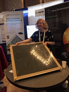
OVERSIZED The author, with Deca Technologies' 600mm x 600mm FO-WLP panel.
Progress in equipment and process methods were also described. Atotech described improvements in electrolytic plating for panel FO-WLP. Semsysco presented its high-speed plating line for vertical glass panel fine-line plating that can be used in panel processing. Besi introduced its large panel size bonder with a reported speed of up to 7,000 units per hour and a local accuracy of 1µm.
Fraunhofer IZM presented research of investigations of thermoplastic bonding materials and release processes focused on reducing die shift and wafer warpage in the eWLB chip-first process. Warpage is a major concern for both round and panel FO processes. IME A*Star presented a detailed study on warpage for FO panel-level packaging using a Gen-3 panel. Unimicron described managing warpage using embedded ring designs.
Packaging for Automotive Electronics
This year’s ECTC included many papers on automotive electronics packaging. Papers included developments in flip chip, as well as FO-WLP. Amkor described challenges in developing an automotive-grade I/O FC-BGA package. Nvidia provided insight into the solder joint reliability for a double-side-mounted DDR module for automotive applications. NXP talked about package material selection criteria for high-temperature automotive applications.
MediaTek focused on the reliability of FO-WLP with an extremely large FO ratio package with low ball-density for ultra-short-range radar applications.
Process Developments
Wafer singulation remains the focus of research to improve the process to reduce stress and cracking, especially in advanced semiconductor nodes where ultra-low-k dielectrics are used. ASM Pacific discussed developments in wafer dicing. Disco Hi-Tech Europe and IMEC described the development of advanced dicing technologies for W2W and D2W bonding. STMicroelectronics provided insight into the use of plasma dicing integration schemes for scribe lane layout and the impact on die strength. Electro Scientific Industries described its ultrafast laser scribe method.
Laser bonding is gaining in popularity. JCET described drivers behind the increased attention on laser bonding in a discussion of chip-package interaction for a fine-pitch flip-chip package for a 7nm semiconductor node die. Pac Tech USA described its vertical laser-assisted bonding for advanced chip-packaging.
IBM Canada and Université de Sherbrooke presented a laser-induced trench design: an optimization that restricts capillary underfill spread for advanced packages.
SiP and AiP
System-in-package (SiP) and antenna-in-package (AiP) solutions continue to receive a lot of attention, especially as the rollout of 5G continues. Intel described an ultra-large SiP and integrated mmW antenna array module for a 5G mmWave outdoor application. Glass substrates for mmWave applications are also seeing increased interest, and a presentation from AGC provided insight into the latest progress. ASE, Samsung and SPIL discussed AiP developments. EMI shielding is increasingly important, and a variety of methods are being introduced. Plating is one process in high volume today. Henkel introduced a compartmental EMI shielding material that is jet-dispensed.
Power Devices
Wuxi Sky Chip Interconnection Technology introduced its embedded die concept for power discrete devices that takes place on a large panel.
Developments in power devices, including new materials for die attach, were highlighted at the conference. Mitsui Mining & Smelting described development of a new Cu sinter paste for low-temperature pressure sintering. Shenzhen Institutes of Advanced Technology also discussed dendritic Cu-based pastes.
Emerging Technologies
Emerging technologies discussed at ECTC include wearable electronics. New developments in printed electronics and additive manufacturing are part of this especially fast-moving area. The lunch keynote by Dr. John A. Rogers, director for the Center for Bio-Integrated Electronics at Northwestern University, was particularly inspiring as he detailed developments in wireless monitoring using soft electronics and microfluidic systems for the skin in neonatal intensive care.
Researchers at Georgia Tech presented work on biosensors with stretchable materials. Michigan State University described a pH sensor for health monitoring. IBM described an RF-connected wearable strain sensor that measures nail deformation from finger movement. Researchers at UCLA discussed a novel heterogeneous integration FO-WLP process based on a foldable display on an elastomeric substrate. National Tsing Hua University and Chang Gung University described development of an inkjet-printed filtering antenna on textiles for a wearable application. Flex and Panasonic detailed a reflow process for flexible hybrid electronics using stretchable film. Reliability of printed electronics is on everyone’s mind, and GE presented an assessment of highly stretchable interconnects for flexible hybrid electronics. Battery technology is important for emerging wearable applications. IBM and Front Edge Technologies described developments in a thin-film battery for healthcare and IoT applications.
With the potential for µLED production, several companies described process developments. Veeco and UCLA discussed the high-yield precision transfer and assembly of GaN µLEDs using laser-assisted micro-transfer printing.
ECTC’s special preconference sessions were Transient Electronics: A Green Revolution for Packaging, Photonics on the Cutting-Edge of Technology Evolution, and Future Visions of Electronic Packaging. A lively discussion took place one evening on unleashing the power of diversity in our workforce. The evening panel session discussed sensors and packaging for autonomous driving. The next night’s session focused on IC packaging materials for next-generation smartphones.
Clearly the industry is entering a new era with the introduction of smart packaging, including heterogeneous integration. Cooperation among various parts of the industry, including design, manufacturing and test, is required to bring these new architectures to market. ECTC is providing the venue for collaboration. Next year’s ECTC should provide even greater opportunities for discussion. The Electronics Packaging Society (EPS) will hold ECTC May 26-29 in Lake Buena Vista, FL, near Orlando.
is president of TechSearch International (techsearchinc.com); jan@techsearchinc.com.
Register now for PCB West, the leading conference and exhibition for printed circuit board design! Coming Sept. 9-12 to the Santa Clara Convention Center. pcbwest.com


