Unequal Ball Size
 Warping during reflow can leave solder balls distorted.
In cases where pad size, solder paste volume and solder spheres on a BGA are consistent in size, the solder joint size variation shown in FIGURE 1 is typically soldering-related. Modern x-ray systems can measure the joint sizes automatically and output a spreadsheet with the data. It is not uncommon to take these measurements on pre-production prototype builds, when product is working. This provides a permanent record of the ball variation on a satisfactory product. If problems are experienced in volume production, the results can be easily compared.

Figure 1. BGA warpage can compress or distort solder balls.
Typically, the reason for joint size variation is warpage of the BGA during reflow soldering. Basically, either the center or the outer edge of the package is depressing the solder paste and sphere that has now reflowed. As the solder solidifies, if the package is still warped (either up or down), it can cause variation in ball size diameter.
Warpage can be specifically related to the component type; some package designs always warp, and engineers need to adjust other parts of the process to accommodate them. Experience shows the die size has an impact, as do the molding compounds used in the packages.
Moisture levels in the components will also affect package distortion during reflow. In the worst case, it will cause the package to popcorn during reflow. If so, the solder may be shorted together due to the sudden compression. In some cases, solder has been seen to eject from under the BGA as solder balls on the board surface.
Dye and pry failure analysis. One method to examine separation between solder and pad on a BGA solder joint is the dye-and-pry technique.
FIGURE 2 is a good example of 90% dye penetration. It shows an optical image of a lead-free BGA solder joint where separation has occurred. The red dye has penetrated between the pad and the solder joint before the package was pried from the board. The image shows where the pad was soldered in place before some mechanical force had caused the separation.
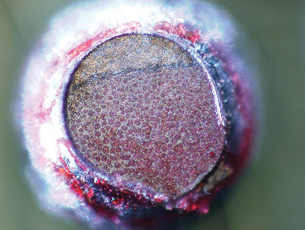
Figure 2. Solder separation on a BGA solder joint.
Red dye is preferred for this investigation, although yellow and blue are available. FIGURE 3 shows a close-up of the dye on the surface of the solder. The dye-and-pry process is useful during failure analysis, process development and is very cost-effective. The test is on its way to becoming an IPC test method (IPC-TM-650, 2.4.53, Dye and Pry Test Method), although with many techniques there are differences in opinion on some of the methods used. A video showing parts being tested can be found at youtube.com/watch?v=P-u2LJd7vSk.
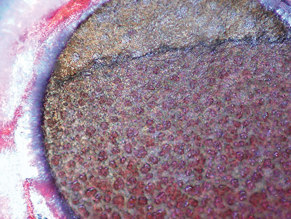
Figure 3. Dye on solder surface.
These are typical defects shown in the National Physical Laboratory’s interactive assembly and soldering defects database. The database (http://defectsdatabase.npl.co.uk), available to all this publication’s readers, allows engineers to search and view countless defects and solutions, or to submit defects online. To complement the defect of the month, NPL features the Defect Video of the Month, presented online by Bob Willis. This describes over 20 different failure modes, many with video examples of the defect occurring in real time.
is a consultant at the National Physical Laboratory (npl.co.uk); martin.wickham@npl.co.uk. His column appears monthly.


