01005 Chip Pad Shorts

Subminiature parts are susceptible to poor board etching.
The smaller the component, the smaller the separation gap, increasing the likelihood of shorts. That’s the case in FIGURE 1. The 01005 chip component footprint with an open solder mask aperture design shows as an etching fault on one of our test boards. We have also suffered from over-etching on boards with smaller features like metric 03015 chip components, which can be a challenge in manufacturing. The short example is a failure in the etching and etch resist part of the process, but should have been captured during AOI.
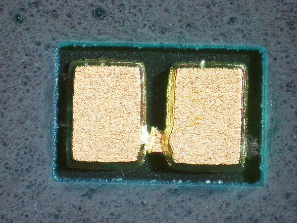
Figure 1. PCB short.
On small features we have experienced nickel foot on laminate and on the solder mask. An example is shown in FIGURE 2. Basically, the nickel is plating onto the surface of the board, away from the pad, which is then coated with gold. This increases the likelihood of solder shorts during reflow soldering, and there has been a marked increase in nickel foot seen on boards the past couple of years.
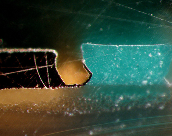
Figure 2. Microsection of nickel foot.
These are typical defects shown in the National Physical Laboratory’s interactive assembly and soldering defects database. The database (http://defectsdatabase.npl.co.uk), available to all this publication’s readers, allows engineers to search and view countless defects and solutions, or to submit defects online. To complement the defect of the month, NPL features the “Defect Video of the Month,” presented online by Bob Willis. This describes over 20 different failure modes, many with video examples of the defect occurring in real time.
is with the National Physical Laboratory Industry and Innovation division (npl.co.uk); chris.hunt@npl.co.uk. His column appears monthly.


