Accelerating the Solder Paste Evaluation Process
A new way to assess up to 25 solder paste properties on an assembly line in five hours or less.
Why change solder pastes? Because defects like solder balls, tombstones, skews, bridges and voids can all be caused by the paste formulation. Process engineers and specialists can try changing stencil designs, padstacks and reflow profiles to mitigate defects, but if the solder paste is not a good match to the process or board design, opportunities for improvement are severely limited. Upgrading to newer formulations has been shown to instantly reduce paste formulation-related defects.1
Why not change solder pastes? The costs of line time, test assemblies and technical resources add up fast. There’s also the risk of overlooking a critical property of the paste and choosing the wrong one for the job, especially because there are no accepted industry test methods to determine paste performance on an actual assembly line.2
The SMTA Test Kit project was developed specifically to address paste-related cost concerns. It is a comprehensive standardized test that gathers information in a time-efficient manner and enables customized, data-driven decisions on the best product for a given process. FIGURE 1 shows the vision of the turnkey test kit.
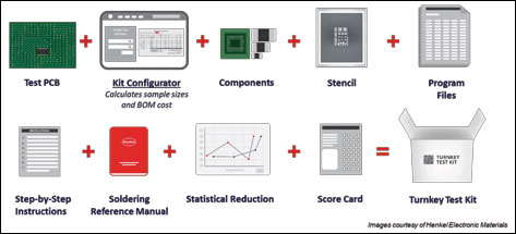
Figure 1. Solder Paste Evaluation Test Kit contents.
Test Vehicle Design
The SMTA Miniaturization Test Vehicle (MTV) is shown in FIGURE 2. The top side, or populated side, contains numerous miniaturized components:
- Eight 0.3mm BGAs
- Nine 0.4mm BGAs
- Ten 0.5mm BGAs
- Four blocks of 008004 (M0201) components (100 each)
- Eight blocks of 01005 (M0402) components
- Eight blocks of 0201 (M0603) components
- Ten 0.4mm MLF components
- Additional 0402s, 0603s and 1206s.
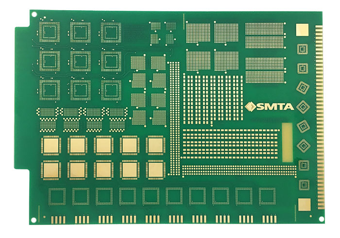
Figure 2. Test PCB top-side.
The bottom side, or unpopulated side (FIGURE 3), contains numerous paste property tests:
- Wetting
- Spread
- Slump
- Bridging
- Fine feature printability (PTF or print-to-fail).
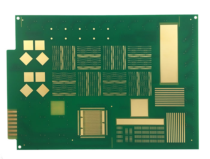
Figure 3. Test PCB bottom side.
Solder paste properties tested. Combining the layout of the PCB and a prescribed, nested test method enables the user to determine any eight of the following solder paste characteristics:
- Transfer efficiency (Cpk)
- Volume repeatability (Cpk)
- Process capability (Cpk)
- Peaking or dog-earring – visual and heights
- Response to abandon time (Cpk)
- Response to stencil life (Cpk)
- Wipe sensitivity (under wipe between prints) (Cpk)
- Hot and cold slump (SPI) – areas
- Tack – visual
- Voiding – BGA and QFN, chip resistors (visual/x-ray)
- Head-in-pillow – BGA, CSP (visual/x-ray)
- Tombstoning – chip capacitor
- Skewing – chip capacitor
- Solder balling and beading – chip resistor (visual/x-ray)
- Wetting to components (visual)
- Wetting to board surface finish (visual)
- Spread on board surface finish (IPC test)
- Coalescence – small components (visual)
- Reliability (SIR, offline, ICT)
- Reflow residue cosmetics (test engineering, offline)
- Cleanability/reliability (ion chromatography, offline)
- Post-reflow materials compatibility (offline)
- Material compatibility (underfills, conformal coatings).
The 20-plus solder paste characteristics that can be evaluated in the test regimen represent the needs of most assemblers. However, special needs can be addressed by modifying the test plan or even the PCB layout itself.
The chart in FIGURE 4 shows how the characteristics are grouped into similar property categories. FIGURES 5 and 6 show the CAD images of the test board and highlight each section of component footprints.
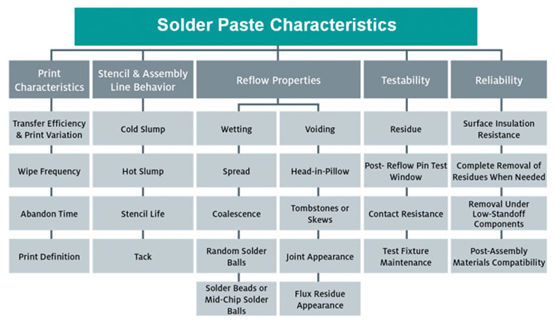
Figure 4. Solder paste characteristics chart.
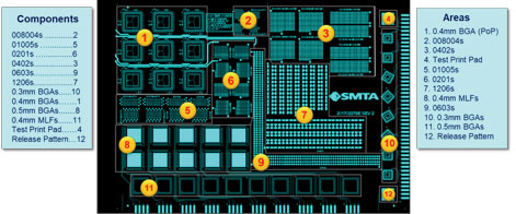
Figure 5. Top (populated) side layout.
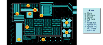
Figure 6. Bottom (unpopulated) side layout.
For users specifically interested in transfer efficiency, the chart in TABLE 1 illustrates area ratios for each land pattern at different stencil foil thicknesses.
Table 1. Area Ratios for PCB Land Patterns at Various Stencil Foil Thicknesses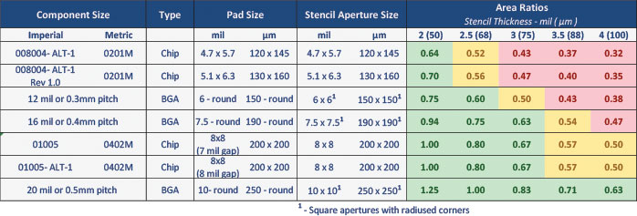
Setup. The documentation package for the test kit includes:
- ODB++ file
- Bill-of-materials (BoM) and sample size calculator spreadsheet
- Stencil Gerbers
- Step-by-step instructions for 30 print design of experiments (DoE)
- Scorecard
- SPI and AOI programs as they become available.
The test board should be no more difficult to program and set up as any new product, perhaps even easier due to the small quantity of part numbers.
BoM and sample size calculator. An Excel spreadsheet displays component numbers and costs from a commercial dummy component provider.3 The actual costs and the name of the provider have been omitted from FIGURE 7, but the actual web download will have the complete cost and provider information.
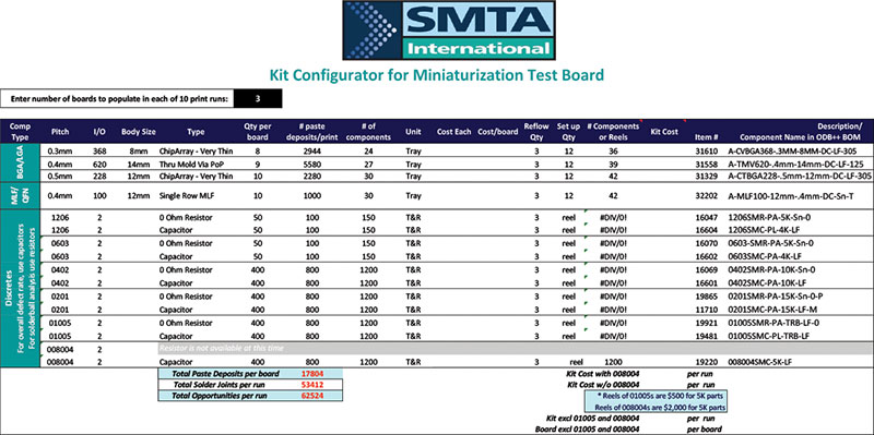
Figure 7. Configurator, or BoM, and sample size calculator.
The calculator provides sample sizes based on the I/O of each component and displays them at the bottom of the sheet. Seeing the sample size and cost together can help make tradeoffs between test materials’ cost and data quantity more transparent.
Test Execution
Designed-in experiments. The PCB’s topside layout has several DoEs embedded in it:
- QFN center pad voiding
- Five aperture designs
- Two replicates (10 components) and overprint on toes, as seen in FIGURE 8
- 1206, 0603
- One variable – vertical or horizontal mounting, user chooses components
- 100 replicates (200 components)
- 0402, 0201
- Three variables – resistor or capacitor, vertical or horizontal mounting, solder mask bridge or no solder mask bridge between pads
- 100 replicates (800 components)
- 01005
- Three variables – resistor or capacitor, vertical or horizontal, different pad spacings (no room for solder mask bridges)
- 100 replicates (800 components)
- 008004
- Two variables – capacitors only, vertical or horizontal mounting, different pad sizes
- 100 replicates (400 components).

Figure 8. MLF aperture designs.
The unpopulated side offers both standardized and original test patterns with the following sample sizes4:
- Slump
- Industry standard test pattern, n = 1
- Internally developed for visual inspection, n = 240
- Internally developed for automated solder paste inspection, n = 60
- Solder ball
- Industry standard test patterns, n = 10
- Spread
- Industry standard test patterns, n = 10
- Internally developed, n = 8
- Internally developed, n = 20
- SIR
- Industry standard test patterns, n = 1
- Fine feature printing, also known as PTF (print-to-fail) patterns
The eight PTF test cells produce 64 mask- or copper-defined circles and squares, and 32 copper-defined rectangles in each direction, with apertures at 1:1 and the same shape as the pad.
Each cell repeats the pattern twice. The top portion prints “squircles,” or radially cornered apertures. The bottom portion prints apertures the same shape as the pads: square, circular or rectangular. This design is meant to demonstrate the effect of aperture design on deposition quality. Solder-mask-defined rectangles were intentionally omitted to utilize the space for better process-indicating features. An example of the test cell is shown in FIGURE 9.
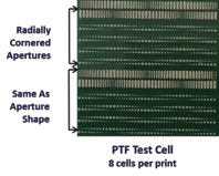
Figure 9. Print-to-fail (PTF) test cell.
The radially cornered apertures more than 8 mils (200µm) wide have corner radii of 2 mils; apertures less than 8 mils wide have corner radii 25% of their width. The area ratios for apertures ranging from 3 to 15 mils are 0.19 to 0.94.
The majority of production facilities will be most interested in the feature ranges of 7-10 mils, or area ratio ranges of 0.44 to 0.63, which represent the demands of the near term on the low end, and a baseline of well-controlled printing on the high end.
More documentation slump, solder ball, wetting and spread test analysis will be included in the next technical paper on this topic.
Maximizing Test Efficiency
To gather the most data with the least resource expenditures, the tests have been nested, enabling the concurrent execution of multiple assessments.
First, the populated side is printed, placed and reflowed. The stencil is then set aside to introduce abandon time tests, and the unpopulated side is loaded up. Boards are printed and reflowed; then the paste gets kneaded to shear it for a fixed time. It is then printed and reflowed again to evaluate its stencil and production line life. After the post-shear run on the unpopulated side, the populated side is reinstalled, and the solder paste’s response to abandon time – or how many prints it takes to return to a steady state and if it reflows as well – is measured. FIGURE 10 shows a flowchart of the test process. A copy of the DoE spreadsheet can be seen in Appendix A.
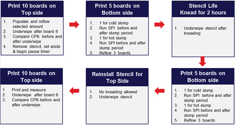
Figure 10. Nested test order.
Data Analysis
A scorecard helps the users customize their paste selection to fit their specific process or product needs. Prior to executing the tests, the user reviews the solder paste characteristics tested on the PCB and determines the relative importance of each to their operation. For example, recovery from abandon time is far less important to a high-volume operation than it is to a low-volume operation that has many stops and starts.
After running the tests and compiling the data, the user then ranks each solder paste’s characteristics relative to each other. The poorest-performing product receives a score of one, and the best-performing product receives the highest score, equal to the number of products in the trial. Typically, four or five pastes are compared at a time. The rest are ranked in ascending order based on their performance. The relative ranking achieves three goals:
- Smoothly blend objective data, like Cpk, with subjective data, such as solder joint appearance.
- Easily compare tradeoffs between different formulations.
- Provide a baseline with the current product and provide insight on what the assembler can expect when introducing a new selection.
The basic categories of solder paste performance include:
- Printability
- Reflow
- Testability
- Reliability
- Supplier support and value.
The scorecard shown in FIGURE 11 breaks each major category into subcategories. Relative solder paste performance for each major category is judged by viewing their weighted subtotals at the bottom line of each section.
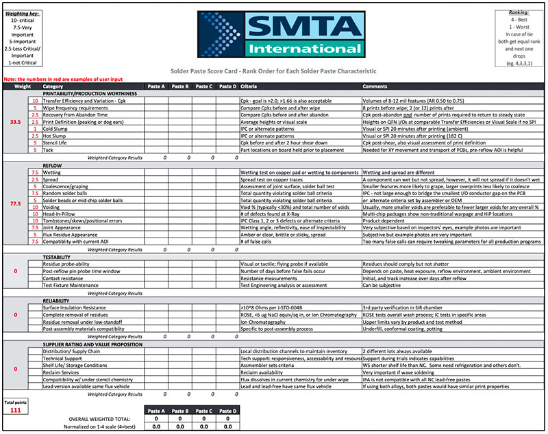
Figure 11. Solder paste evaluation scorecard.
Complete weighted totals are shown at the bottom of the sheet. Typically, the best performer is the solder paste with the highest overall score. Sometimes, however, the runner up takes the prize. The highest scorer may have a disappointing flaw – such as high voiding, solder balling, graping, peaking, or low wipe frequency – that can’t be tolerated.
It is not uncommon for a solder paste’s performance to be great in one category, yet mediocre, or even weak, in another. Solder paste characteristics are balanced during formulation, where often a particular characteristic is optimized. Even most successful products have performance tradeoffs.
SMT operations also have their strengths and weaknesses. Therefore, finding the optimum solder paste for a specific process requires investigation of the properties most critical to the operation. The scorecard provides a data-driven method for examining and comparing such properties.
Summary
The intent of the test kit concept is to make solder paste testing fast, easy and as straightforward as possible. All the pieces of the kit were designed with ease of use in mind. The common test vehicle will enable different users to compare experimental results, leading to faster process development and dissemination of knowledge.
Future Work
A website where experimental results can be uploaded, and essential files for testing can be downloaded, is currently under construction. Downloadable files will include:
- Kit configurator, or BoM cost-sample size spreadsheet
- Stencil Gerbers
- Pick-and-place files
- ODB++ files
- Scorecard.
The finished website will be accessible from the SMTA website (smta.org). Until then, files can be obtained by emailing the author directly. The website is expected to host uploaded experimental results. Investigators will be able to share, review or post suggestions in a discussion forum, which will also be on the website. Additionally, PCB support tooling has been designed for MPM, DEK and EKRA printers and is available via a printer tooling manufacturer.5
Availability. As of February 2019, the first production lot of PCBs is on order and will undergo a first article inspection prior to commercial release. The kit’s elements are complete, except the reference manual and publication of the statistical methods.
Based on the best information at the time of publication, PCBs should be available by the beginning of April 2019, and website shortly thereafter. The reference manual and statistical methods are anticipated to be available online by late summer 2019.
References
1. R. Lawrence and C. Shea, “Solder Paste Qualification Testing for EMS Production,” SMTA International Conference Proceedings, October 2017.
2. Results of online poll of SMTA webinar attendees during presentation of the test kit, March 2018.
3. Practical Components, Los Alamitos, CA.
4. D. Dixon, et al, “Development of a Solder Paste Test Vehicle for Miniaturized Surface Mount Technology,” IPC Apex Expo 2018 Proceedings, March 2018.
5. Rapid Tooling, Plano, TX.
Ed.: This article was originally published in the SMTA International 2018 Proceedings and is republished here with permission of the author. Appendix A, Nested Solder Paste Evaluation Steps, is available online.
is founder of Shea Engineering Services (sheaengineering.com) and a three-time best paper winner of SMTAI; chrys@sheaengineering.com.


