Understanding PCB Design Variables that Contribute to Warpage during Module-Carrier Attachment
A DoE of laminate, copper balance and panel configuration.
A WiFi module was soldered to one of several different product-specific carrier PCBs. The module is an eight-layer ELIC PCB, 30 x 40mm and 0.77mm thick, fabricated with a mid-Tg, halogen-free laminate. The module has an LGA pattern with 333 pads 0.6mm2 and ENIG surface finish. There are several configurations of carrier boards, but all are 1.57mm thick with immersion silver finish. FIGURE 1 shows the LGA pattern of the module, the corresponding pattern on a representative carrier board and the assembled module-carrier system.
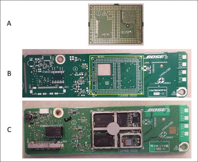
Figure 1. WiFi module LGA pattern (A), corresponding LGA pattern on a representative carrier board (B) and assembled module-carrier system (C).
Shortly after product launch, solder opens between module and carrier interconnect were detected at ICT. Assemblies were failing at a 50,000ppm defect rate. Prying the module off the defective assembly revealed there had been no solder contact between the module PCB and paste on the carrier pads on the lifted corner of the module (FIGURE 2).
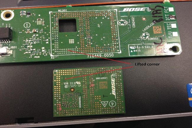
Figure 2. A failed module-carrier assembly after separation showing no solder on the pads in the lifted corner of the module.
The module is assembled in a conventional SMT process building the bottom side first, followed by topside assembly. The module and carrier boards are SMT-only designs with no through-hole components. The module was panelized in a six-up array and the carrier in a four-up. Several critical components on the module were type 3 moisture-sensitive devices with an exposure limit of 168 hr. Since the module would be soldered to the carrier as an SMT device, it is critical it be handled as an MSD once assembled. To avoid baking, exposure times are tracked during subsequent test processes and stored in dry boxes. Once tested, the module is routed and placed into Jedec matrix trays with desiccant packaging and placed in stock until needed for assembly to the motherboard.
It was recognized in early prototypes that maintaining PCB flatness during the process would be an important factor for successful soldering of the module to the carrier. This led to a decision to use process carriers for both the module and carrier. FIGURE 3 shows a typical SMT process carrier. For the thinner module, the pallet would be a significant process enhancement, providing solid board support for printing and placement. For the carrier, the pallet was primarily to control board sag common during the double-sided reflow process.
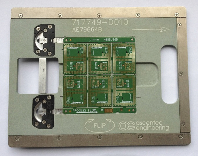
Figure 3. Module panel in process pallet.
Fishbone Analysis
A team was formed consisting of the plant supplier and process quality, plant process engineers, corporate manufacturing engineers, design engineers and the PCB commodity engineer to analyze the problem following a DIMAIC (define, measure, analyze, improve and control) methodology. A key part of that process is to develop a cause-and-effect diagram outlining the process to identify potential areas having an influence on the defect (FIGURE 4).
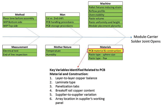
Figure 4. Cause and effect diagram.
The team evaluated each item in the diagram, performing process audits for MSD processes and work methods, analyzing data for environmental control and analysis of process parameters. The oven profiles were checked to the paste supplier’s recommendation, and no variations were found. The modules were thermocoupled in the four corners and center during the carrier assembly process and were found to be within 1.5°C across the part.
Module panels were checked for flatness using the methodology in IPC-A-6101. The modules were found to be within the 2mm allowed for a panel this size. For the module, this would translate to a 0.75mm warp. The IPC standard would be fine for assembly of a regular PCB but was not tight enough to solder an LGA into 7 mils of solder paste. Considering specifications for BGA packages would be more applicable, the JEITA specification on BGA package warpage2 was referenced. The specification for FLGA packages was found to roughly fit the module. The 1.27mm pitch was larger than the 0.8mm maximum pitch in the table, but the trend for all the devices was the maximum warpage could not exceed the height of the molten solder on the component site. Realizing this specification would be too tight for the PCBs on hand and would adversely affect the material, the team decided to use the 0.177mm (0.007") paste height as the standard.
A jig was developed to hold the modules, and they were to be inspected using a go/no-go shim before packaging into trays. While evaluating the raw panels, it was observed approximately 10% of those received were severely warped. To increase yields of finished modules and avoid scrap, a sorting process was developed for the raw panels. Panels would be sorted into three categories: A <0.5mm; B >0.5mm, <1mm; and C >1mm. Only group A PCBs would be built. With these controls in place, the defect rate for unsoldered modules dropped, ranging from lows of 2,000 to 10,000ppm.
With a containment plan in place, the team began working on areas of the fishbone to discount noncontributing factors, improve board flatness and adjust process variables to improve yields. Baking boards did not improve flatness. Boards baked with weights to flatten the panels improved to acceptable levels but relaxed to their original condition over several days. Increasing solder paste height and volume did not significantly improve the process and began to produce shorts. Profile adjustment had no effect. Several samples of the module and carrier were sent out for shadow moiré analysis. The evaluation determined the PCBs were changing during reflow processing, with the module warping upward (smiling) and the carrier warping downward (frowning). It became clear the board stability needed to be improved. The team met with technical resources from the two board suppliers and discussed PCB variables that could affect flatness. The major potential contributors identified were the material selection and copper balance. Less impact was expected from process changes at the supplier. Those changes included baking under pressure and better flatness sorting techniques. While the suppliers developed proposals for different materials, the design team investigated changes to copper balance and the panel design. FIGURE 5 shows the existing and proposed copper balance.
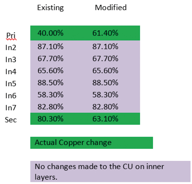
Figure 5. PCB copper balance.
One observation was that while the module copper had etches and reliefs, the rails had unbroken planes. This is commonly done to stiffen panels and prevent sag during the reflow process. The team questioned whether it might impart stress during heating or in the lamination process. Another observation was corners where defects occur were not tied into the panel. Breaks had been placed in the center to minimize tabs and reduce routing time. The final attribute the team felt might be significant was the fabricator’s working panel position. The assumption was modules from the corners of the working panel would have a greater warp than those from the internal portions of the sheet.
Experimental
Upon completing the cause-and-effect analysis, the team designed an experiment to answer the two main questions coming out of the evaluations. First, was variation in the process causing defects, or was PCB flatness the defining factor?
Despite the experiments and evaluations, the measurement capability limitations left this question unanswered. The process was demonstrated to be in control and followed convention with regard to printing placement and reflow parameters. The second question focused on the raw PCBs: Which changes made to the materials and designs would have the greatest impact on PCB flatness?
Phase 1 of the experiment would measure the full population of PCBs in groups A, B and C at each process step to determine whether the boards were changing as they were processed and by how much. Working with our statistical engineer, the board quantities needed (TABLE 1) for a valid experiment were determined and a matrix designed. Panels from each of the A, B and C groups would be run to verify whether the initial board warpage was the leading factor in solder opens or if the process had a significant impact.
Table 1. Phase 1 Sample Allocation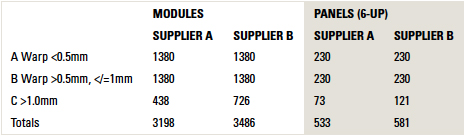
Phase 2 of the experiment would involve the same measurement strategy as phase one, using PWBs implementing the material and design changes the team wished to investigate. Attributes to be studied were the materials, panel position, copper content of the rails, board break quantity and position, and copper balance. Each supplier had a different recommendation on material. Supplier A recommended a BT core with the existing material used for the cap layers.
Supplier B recommended a different laminate they felt was more stable. TABLE 2 shows the PCB quantities by attribute and supplier.
Table 2. Phase 2 Sample Allocation (by 6-Up Panel)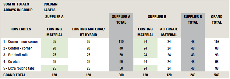
With the build matrix designed, it was found cost for multiple variations of the PCB would add significantly to the budget of the experiment. In an effort to reduce fabricator setups and individual types required, variations were combined into a single working panel, with different panel locations having different attributes. The new material variations and existing material controls would be built using the same working panel designs. Each supplier had its own working panel size, so a separate but similar layout and matrix were made for each. FIGURE 7 shows one of the supplier’s working panels. TABLE 3 shows the key to the variations in the working panel.
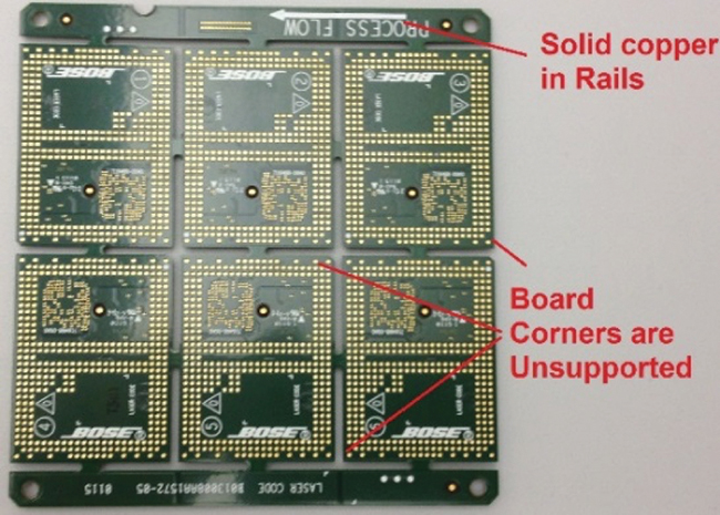
Figure 6. Module rails and break tabs.
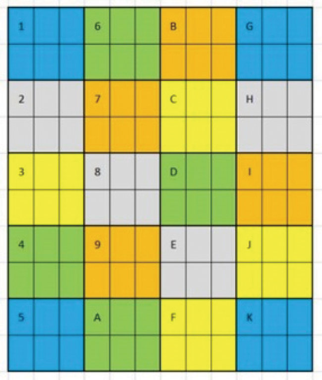
Figure 7. Working panel for supplier 1.
Table 3. Working Panel Variant Key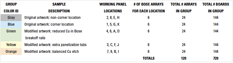
Measurement needs and method selection. While designing the experiment, the team became concerned with the large number of measurements needed. With plans to measure 1,654 module panels three times and 2,481 carrier panels, resources would become a problem. Splitting the measurements into individual boards would yield 39,696 pieces of data for analysis. TABLE 4 illustrates the labor hours for three automated measuring strategies. Selecting the correct measuring method was critical for success. The quantity of modified PCBs for the phase 2 portion of the experiment was limited to one run, leaving no opportunity to recover from mistakes or corrupt data. The team looked numerous ways to collect data and found each with drawbacks. Automated methods would be costly in equipment and technicians, but manual methods would be costly in speed and accuracy. The following paragraphs describe the advantages and disadvantages of each option considered.
Table 4. Measurement Time Comparison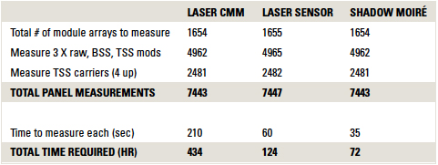
Use only test pass/fail data. This method would not measure boards at all, but use only the A, B and C classifications for phase 1 and the attribute change groups for phase 2. While fast and low cost, this was deemed unacceptable. This method would produce no process insight, and given the low defect rates, there would not be enough information to identify trends and draw any meaningful conclusions.
Hand measuring with pins and gauges. This was the method currently in use. This could be implemented quickly, but measurement was slow and results subject to variability of the operators. The precision would also be low. It was decided this method would not produce the information needed for sound conclusions.
In-house laser CMM. Measuring would be done using a system located in the corporate R&D center. This method would produce the quality of data needed for success and used existing resources. The disadvantages of this method were the long measuring time of our system (3.5 min.), the lab hours required (400 hrs., which would be charged to the project), and the logistics of shipping boards between corporate on the East Coast and the plant on the West Coast. These factors combined to make this an undesirable option. It was also considered that long stretches between measurement and further processing could make the information unrepresentative of the existing process, where boards are completed in two to three days.
Use a metrology contractor near the plant. To counter logistics issues of shipping boards to the corporate lab, the team searched for a metrology lab with similar capabilities local to the plant. It was assumed the cost and measuring time would be similar, which would still be a disadvantage. No suppliers were identified for this volume of measurement, so this option was discounted.
Purchase a laser CMM for the plant. This option would mitigate the disadvantages of using the corporate lab equipment and would provide additional capability locally to production. Plant labor could be used at a lower rate, and additional shifts are available to perform measurements within the schedule. The disadvantages of this option are the cost of the equipment ($85,000 to $90,000), the lead time and training to set up the equipment, and the justification and approval cycle required for capital equipment. The lead time and cost of this method eliminated it from consideration.
Develop an in-house measurement system. The team identified a linescan laser sensor that could quickly take precise measurements. The supplier also offered data analysis software. With an in-house equipment design group and a precision gantry workstation available, this seemed like a low-cost alternative that could be implemented quickly using existing resources. The equipment group estimated a cycle time under one minute, an improvement over the laser CMM in the lab.
This system would enable colocation of the equipment on the production floor. Measurements would be taken between board sides within the cycle time of the SMT process, thus ensuring the measurements taken were representative of the process as it is run on a daily basis. After working with the sensor and software, it was found the program development time was far more than initially thought. Engineering labor costs were estimated at $18,000. With the purchase of the sensor, the project would cost over $28,000. Being a development project, it was likely there would be bugs at the startup of the equipment. This presented a significant risk to the project if the data were corrupted or lost. This alternative was put on hold to investigate several of the other options described above.
Lease a shadow moiré. Having run an evaluation during our investigation of likely defect causes, the team had become familiar with its capabilities and had maintained a relationship with the manufacturer’s representative. While discussing further testing, it was suggested leasing the shadow moiré might be a viable option for the project. The equipment could be used without the heater for a quick cycle time. With a measurement time of less than 2 sec. and data density of ~250µm per data point, a large, dense amount of data could be captured to fully characterize the surface shape of the modules’ and carrier boards’ interconnect area. The equipment would also collect the entire board topology, whereas many of the previous options were point-to-point or scanning techniques that have significant tradeoffs between data density and measurement time. The equipment was a fully developed production system with user software tools for data analysis further reducing risk and analysis time. The supplier would provide on-floor training and support for the startup. While the costs were similar to the in-house development project, the risk was far lower and the capability significantly greater. Given its advantages in many areas and the technical support available, leasing the shadow moiré was chosen as the best option for this project.
Shadow moiré overview. Shadow moiré is a noncontact, full-field optical technique that uses geometric interference between a reference grating and its shadow on a sample to measure relative vertical displacement at each pixel position in the resulting image. FIGURE 8 provides a visual diagram of the process. It requires a Ronchi-ruled grating, a white line light source at approximately 45° to the grating, and a camera perpendicular to the grating. A technique known as phase stepping is applied to shadow moiré to increase measurement resolution and provide automatic ordering of the interference fringes. This technique is implemented by vertically translating the sample relative to the grating.
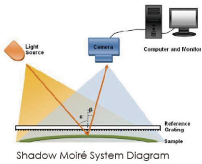
Figure 8. Shadow moiré process visual.
As discussed, shadow moiré offered several distinct advantages compared to the other measurement methods considered. With a measurement time of less than 2 sec., and data density of ~250µm per data point, a large, dense amount of data could be captured to fully characterize the surface shape of the modules and carrier boards. In addition to the interconnect area coplanarity value, it was thought measuring the module-board height after final assembly would also be a useful data point. This was not possible, however, as shadow moiré has a maximum step height measurement capability of ~50 to 100µm.
Although typically used for at-temperature characterization of parts/assemblies, the tool could be adapted to measure the thousands of parts needed for this study. After some fixture modifications and operator training, a scan time of roughly 35 sec. per panel was achieved. This process involved some overhead that would not be needed in a more simplified, room-temperature-only tool. Parts were tracked via serial number for later correlation. Data for the entire panel were taken all at once and partitioned into smaller regions in post-processing. A workflow diagram of the measurement process is shown in FIGURE 9.
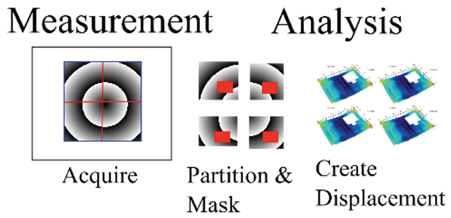
Figure 9. Data processing steps.
Results
Phase 1. The purpose of Phase 1 was to determine whether PCB flatness was the most likely root cause in solder opens at the carrier assembly. Only five of the six A, B and C groups could be built. Supplier 2 had recently been discontinued as a supplier, leaving no Group A from them in stock. Modules were all 2D-laser barcoded and measured in the shadow moiré before use. They were then measured again after bottom- and topside SMT assembly. All measurements were collected at the panel level and data then processed to crop it into individual modules. An automated coplanarity analysis was then run and histograms created for each group. The plots in FIGURES 10 and 11 show coplanarity distribution in microns on the x axis and the percentage of modules at each measurement on the y. With the data broken down into individual boards, measurements were not as concentrated as expected. Each group had a similar distribution of boards in the higher ranges, regardless of its level in the hand-sorting process. After processing, the coplanarity had shifted 60µm higher with no measurements lower than 90µm. The percentage of measurements in the lower warpage region also shrunk from 25 to 35% in the unprocessed boards to 15 to 20% after processing.
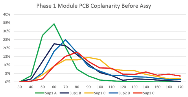
Figure 10. Unprocessed module measurement distribution.
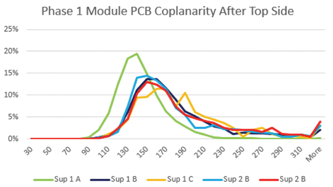
Figure 11. Post topside module measurement distribution.
With the process data showing the boards changing during the processes, it was decided to run an additional analysis of boards at processing temperatures using shadow moiré. A module and carrier panel were sent to the equipment supplier and characterized at temperature to analyze thermal warpage effects that can impact solder joint formation. Warpage values vs. temperature were graphed and gap values between the two surfaces also analyzed. This gives an idea of how the two parts are moving relative to one another in the reflow oven.
Given the paste thickness was roughly 165µm, and this collapsed to roughly half that height at liquidus, a gap fail and warning map was created at 82µm and 50µm, respectively. After analyzing the four-up carrier panel and six-up module panel, statistical surfaces representing the part behavior at eleven temperature points were created. FIGURES 12 and 13 show the average and maximum case at peak temperature, respectively. Gap failures were noted prominently in one corner and correlate well with open failures seen in production.
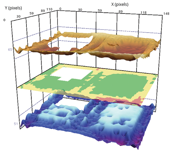
Figure 12. Average plot at peak reflow temperature.
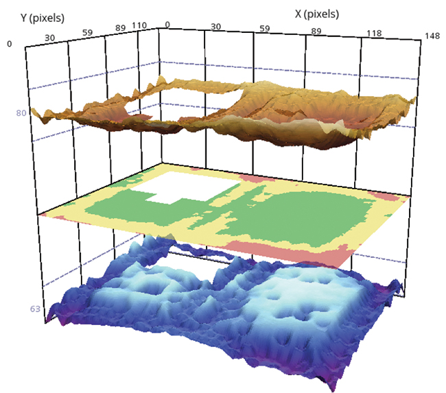
Figure 13. Maximum plot at peak reflow temperature.
Gap vs. temperature plots condensed the surface plots above into a broader picture of the assembly gap behavior over temperature. Three cases were analyzed: the maximum gap across the sample surface, the average gap, and the 3-Sigma gap (average gap plus three standard deviations based on the gap distribution). In addition, two different statistical surfaces were analyzed: average and maximum. These surfaces represent the average of the input surfaces and maximum of the input surfaces, respectively. In this case, there were four real bottom surfaces from the carrier panel, and five real top surfaces from the module panel, that made up these statistical surfaces. Looking at the gap vs. temperature plots in FIGURES 14 through 16, the fact that the maximum gap and 3-Sigma gaps were so similar indicates the surface shape distributions were very close from part to part. Indeed, the individual surface signed warpage values in Figures 14 through 16 show the samples were typically within 10-15µm of each other. Based on these two panels’ behavior at temperature, and the typical paste height described previously, it could be assumed the maximum gap values typically exceed this paste height at peak reflow temperatures. Of course, this ignores the paste’s surface tension and elasticity, but with less well behaved input carrier/module surfaces, the gap values could get quite large.
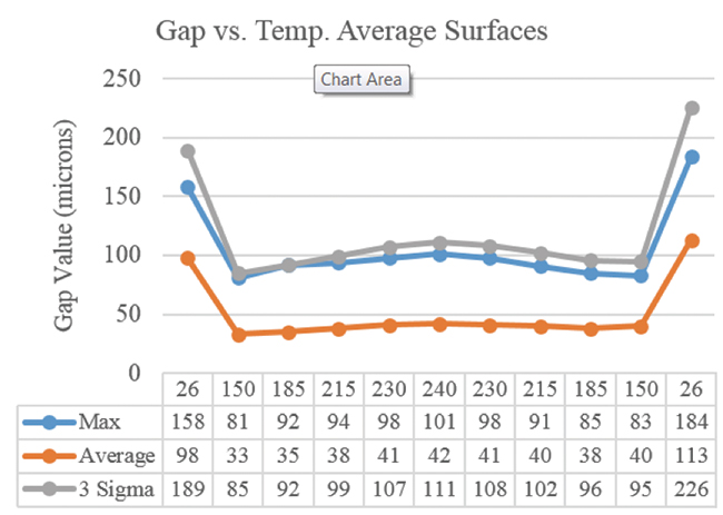
Figure 14. Average gap vs. temperature.
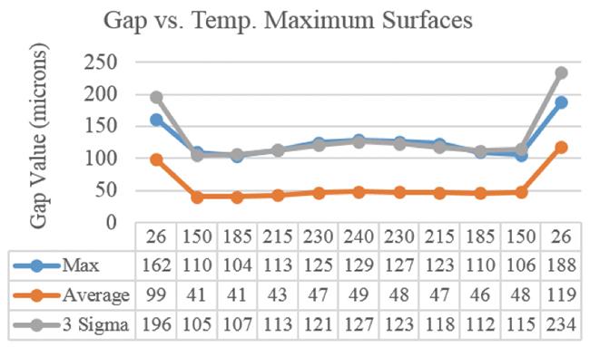
Figure 15. Maximum gap vs. temperature.
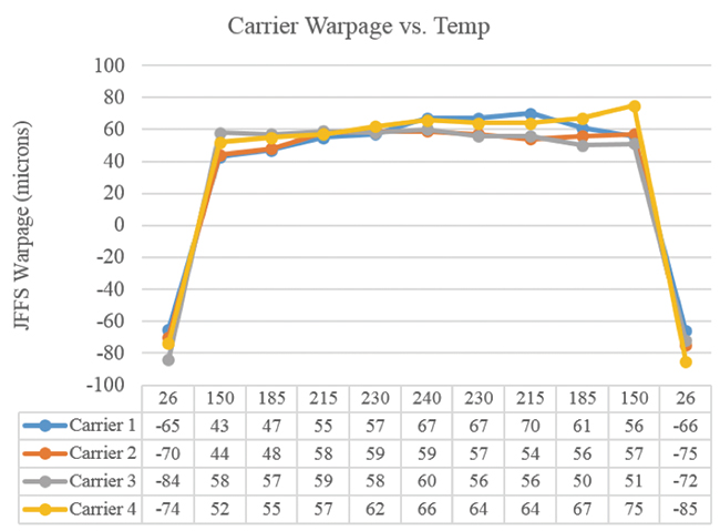
Figure 16. Carrier warp vs. temperature.
While it was clear the boards were warping further during processing, the relationship that coplanarity had on failures in production still needed to be confirmed. The actual ICT test failure rate by board suppliers and groupings were compared (TABLE 5). The failure rate of Group A boards from panels measuring under 0.5mm was very good at 513ppm. As the initial warpage increased in groups B and C, the PPM levels increased significantly, indicating incoming panel flatness did have an effect on the process yields.
Table 5. Test Failure Rates by Group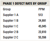
To analyze whether there was a difference between suppliers or position in the module panel, contingency tables were created to compare these attributes (TABLE 6). The supplier table initally indicated the supplier was a factor, but further analysis of the data shows the absence of supplier 2 Group A boards underrepresented supplier 2 so that analysis was not used. The team had originally theorized the corner boards of the module panel would be the least flat. Analysis of the board position revealed there was no relationship (P-value >0.05) to individual module position in the panel and the likelihood of failure. Comparing the coplanarity averages of the failed modules with those of passing modules, there was a difference between them (FIGURE 17).
Table 6. Analysis of Board Position in Panel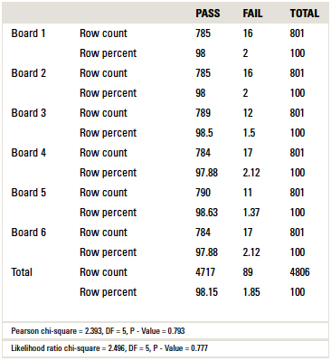
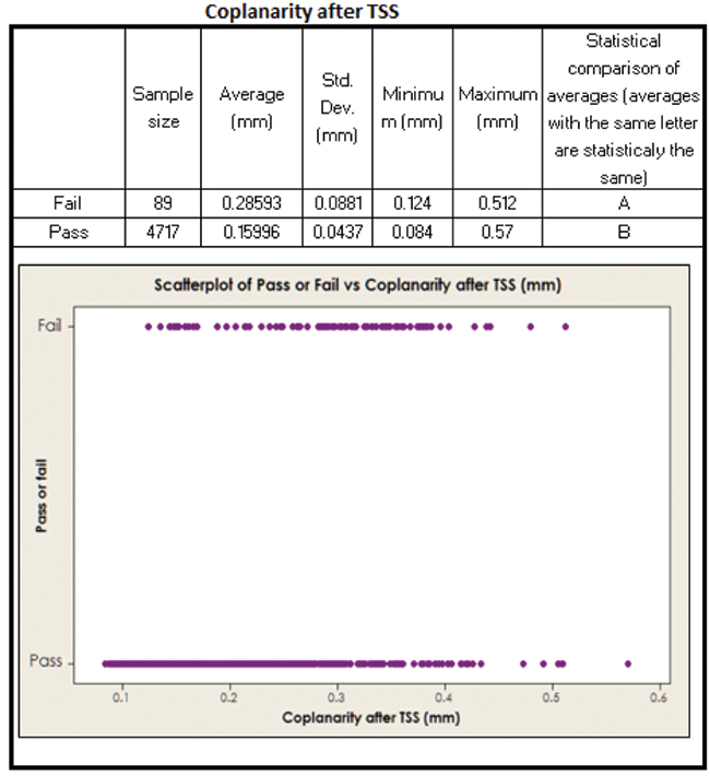
Figure 17. Defect relationship to coplanarity.
Running a logistic regression analysis to determine the likelihood of defects at a given flatness revealed the defect rate could be predicted and there was a relationship between flatness and board opens at carrier assembly. The graph in FIGURE 18 shows that at 0.177mm coplanarity, there is a 1.08% chance of a solder open defect. This correlates closely with the production yields of 1% less defects.
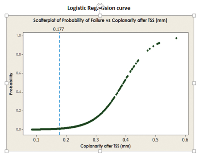
Figure 18. Failure probability curve.
Phase 2. Phase 2 of the experiment was designed to evaluate changes in the design and materials for improved PCB flatness and stability in the process. PCBs were not sorted into flatness groups (as was done in phase 1); instead, all boards from the process were used as-received. There were 20 groups planned for analysis, with variations of the materials and design changes. TABLE 7 describes the attribute groups with the changes and materials used for each. Groups E and J from supplier 2 were not received in time and were left out of the evaluation.
Table 7. Phase 2 Attribute Groups
Analysis was begun by comparing the coplanarity of each variation and looking for the best flatness and least variation. From the raw board data, clear indications were one variation might be better than the others. Once data for processed boards were analyzed, the leading candidates changed. This occurred after both bottom- and topside assembly. Results of the analysis after top side are shown in TABLE 8 and graphed in FIGURE 19. After topside processing, groups K, N and O showed the best resulting average coplanarity. These variations were all from supplier 1 and used the existing material. Group K was from a working panel non-corner; Group N had the additional board breaks at the corners, and Group O had balanced copper top and bottom.
Table 8. Post Topside Coplanarity Measurements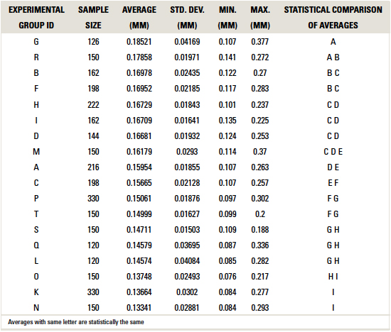
Figure 19. Plot of average flatness by group.
A plot of coplanarity averages for passing and failing boards revealed passing boards had a smaller average and standard deviation but also had a significant number of points outside the box (FIGURE 20). This would make it difficult to point to a specific coplanarity as needed to produce a passing result.
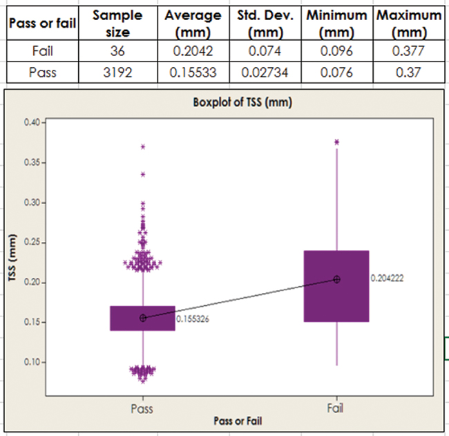
Figure 20. Plot of coplanarity vs. test result.
The second part of the analysis was to match ICT test results with each of the variations to see which actually had an effect on the outcome. Contingency tables were created for comparing variations based on build quantities and failures. A Pearson Chi Square analysis was run on each. The results showed the suppliers, board materials and rail copper variations had no statistically significant association with failure rate. Despite showing better performance in one of the groups for flatness, the copper balance in the PCB showed no difference between existing and modified boards.
The two attributes found to have statistically significant association with failure rate were the position in the working panel, where boards from the non-corner panels showed a higher yield, and the change to the board breaks, where modules with additional breaks moved to the corners had no defects (TABLES 9 and 10).
Table 9. Analysis of Panel Position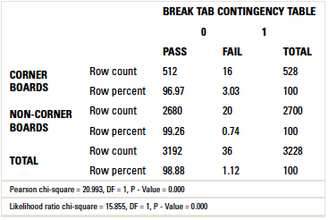
Table 10. Analysis of Board Tabs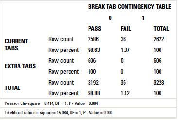
Conclusions
Phase 1. The evaluation determined incoming PCB coplanarity had an impact on yields of the assembly of the module to the carrier. Panels sorted into group A demonstrated a lower ppm defect level than those in the B and C groups. The ppm defect levels rose significantly in Group B and nearly doubled in Group C. Group A had a lower average coplanarity than those in Groups B and C. Despite the sorting at the panel level, Group A still had individual modules with high-coplanarity values but at a lower percentage than the other groups.
In analyzing passing and failing modules, PCB coplanarity was found to have a statistical association to process yield. Passing modules were found to have a lower average coplanarity than failing modules. To improve yields and eliminate board sorting, improvements need to be made in the fabrication process by changing the design or material, or a combination of both.
Phase 2. Despite consensus from PCB suppliers and the product development team, the PCB material and copper balance had no statistically noticeable effect on the assembly yields. The balanced copper attribute may have been underrepresented due to the loss of the Supplier 1 samples and may warrant further investigation. The board position in the working panel was found to affect failure rate. Boards from non-corner locations displayed a better average coplanarity than those from the corners. This attribute may be difficult to change, but will be investigated with the PCB suppliers.
Boards with more tabs located in the PCB corners were seen to have the largest impact on carrier attachment success. Being a simple change to the panel, this change can be easily implemented and monitored in larger lot sizes.
References
1. IPC-A-610D, Acceptability of Electronics Assemblies, section 10.2.7, November 2004.
2. JEITA ED-7306, “Measurement Methods of Package Warpage at Elevated Temperature and the Maximum Permissible Warpage,” section 3.6, March 2007.
Ed.: This article was first published at SMTA International in September 2016 and is reprinted here with permission of the authors.
is manager manufacturing engineering, Automotive Systems division; is component engineer; and Rafael Maradiaga is statistical engineer at Bose (bose.com); donald_adams@bose.com. is applications engineer at Akrometrix (akrometrix.com); rcurry@akrometrix.com.


