2005 Articles
Feinfocus' WBI-Fox X-Ray
Dynamic void detection in wafer bumps, without gray level definition.
The WBI-Fox x-ray inspection system, a precision x-ray inspection system designed for wafer manufacturing, addresses void detection in wafer bumps.
Traditionally, fabricators have employed standard QA inspection tools for the detection of surface anomalies such as scratches, nodules, pits and contaminants. However, these inspection tools cannot look inside solder balls for defects such as voids. Operators pass or fail dies based on judgment, or simply reject dies containing voids. Nevertheless, voids do not necessarily imply defective bumps. Chips may be rejected unnecessarily, while “passed” bumps containing voids could result in poor interconnects. The WBI-Fox views voids in solder bumps and automatically measures void size relative to bump diameter and volume.
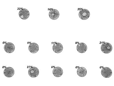 |
| The processed x-ray image shows the diameter percentage of voids detected relative to the total diameter of the wafer bump. |
The system analyzes solder bumps on wafers. It detects voids and determines whether they degrade the viability of chip interconnects. The system accommodates both 200 and 300 mm wafers, and features an automated handling subsystem. It maps the layout of dies on the wafers, selects chips to be inspected, calculates and analyzes void data, determines “pass or fail,” stores images of defective solder bumps and generates reports.
The machine is fully programmable and can incorporate a multifocus tube of up to 160 kV. Besides a wafer handler, the system provides a load port including aligner, a four-axes manipulator, CCD camera for visual wafer tracking, a graphical user interface modified for wafer bump inspection, flat panel screen with status and operation control windows, and software for automated inspection using stored recipes.
The WBI-Fox also features TXI (true x-ray intensity) control, which ensures a constant, controlled level of intensity for consistent x-ray images. Unlike techniques that attempt to maintain image intensity by controlling input parameters, TXI automatically controls the output level of x-ray intensity for constant contrast and brightness and superior image quality.
The FGUI offers standard and configuration modes for solder bump inspection. The standard mode lets operators perform inspection and analyses with preconfigured recipes. During inspection, the operator can monitor any progress on the wafermap for the wafer being x-rayed. In the configuration mode, the process is more detailed. The recipe configuration wizard prompts the operator through a set of procedures for creating a new recipe or editing an old one. Operation control and status windows are replaced with another set of windows, including a WBI configuration screen. These are used to specify the properties of the wafer being inspected, to set the required controls for x-ray imaging, and to create a new wafer layout or edit an existing one after inputting a file with layout information.
Fiducial marks are established for the inspection process with x and y parameters. Once the recipe is configured for the wafer(s) being inspected, it is stored for future access.
Inspection of solder bumps culminates with the detection, measurement and analysis of voids. Essential to determining the viability of a solder bump with a void is specifying a percentage threshold above which the bump can be considered defective. Traditional x-ray systems establish thresholds using static, pre-set grayscale values. The WBI-Fox features dynamic void detection with inspection independent of gray level.
Two options can determine the viability of a solder bump. One is to compare the area of all voids within the total area of the bump in the image to ensure that the threshold is not exceeded. The other compares the largest void diameter within the ball diameter. One of these options must be selected prior to running the inspection program.
During inspection, solder bumps are deemed acceptable (capable of providing a reliable and sufficient interconnect) or unacceptable, depending on the pre-established parameters. The inspection ensures solder bump integrity while reducing the scrapping of viable components due to minor voids.
Micha Lehnigk is in software development at FeinFocus (feinfocus.com); m.lehnigk@feinfocus.com.


