

Century Circuits
 Which PCB technologies are best suited to survive 100 years?
The Goal: Build an electronic device that will outlast everyone currently living on Earth. Looking back 100 years, few of us were here and the same will be said in the year 2124. Just reflecting on the brevity of life but we will take a century as forever.
One hundred years ago – 1924 – was the year that the Computer-Tabulating-Recording Company rebranded itself as IBM. Electric blenders, vacuum cleaners, traffic signals and television are among the inventions of the period. Two inventors of the era were leading us toward printed circuit boards though their patents were not commercially successful. Time would prove them to be quite insightful.
Looking back to move forward. PCBs finally took hold around the middle of the century while integrated circuits followed another 25 years later. My "forever" board is going to make use of these early transistor-to-transistor logic (TTL) components that predated complementary metal-oxide-semiconductor (CMOS) technology. The physically larger transistor gates and the 5V logic are a concern. Both types were used on the Voyager space probes to build the guidance and other systems. There was also a fully discrete version of the computer as a backup to the backup. I have confidence in those old Texas Instrument parts.
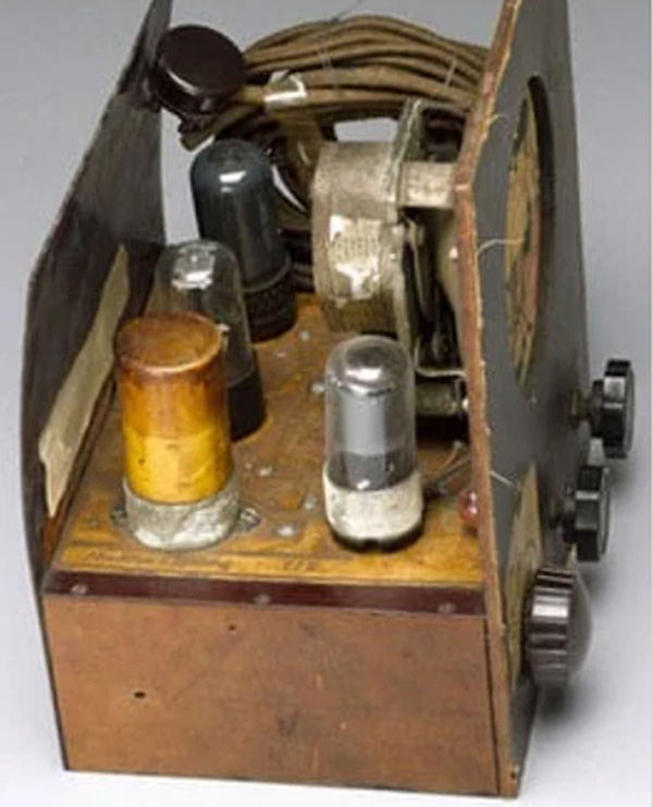
Figure 1. Created by Paul Eisler, the first printed wiring board used for a radio is about 80 years old. (Source: History-Computer.com)
The dual-inline-package (DIP) comes in two flavors. One family's device designation starts with 74 and the other one starts with 54. The numbers indicate the type of package, with 74 being for plastic and 54 representing the same circuit in a ceramic package. Of course, the ceramic parts are what's exciting here. What we know of many lost cultures comes down to their pottery shards and burial sites.
The solid-state technology from the 1990s, while vintage, can still be found. The ceramic leadless chip carrier (CLCC) devices of the day would have a little more integration and could be accommodated on a robust through-hole printed circuit board. If we're not concerned about size, lead time or price, custom devices can be created from more modern chips. Instead of ultra high-density interconnect, we would have single-core processors in packages with a pitch of perhaps 1.27mm.
Finding things that are designed to last. High reliability doesn't have to mean antique technology. The stuff going on in the silicon photonics area includes hermetically sealed modules and devices. Enclosures with SMA connector feedthroughs and laser-welded seals are designed to keep working in almost any condition.
The automotive industry in particular specifies the most resilient connectors. It has made over a century's worth of improvements to the wiring of critical systems. The medical and aerospace industries have ruggedized devices that deserve a look as well. We want to keep our options open.
Metallization for the ages. The lesser-known Copper Age slots between the Stone Age and the Bronze Age. That makes the conductor of choice pretty easy. I'm going to want three to four ounces of copper per square foot on each layer. Yes, that will force wide air gaps on my four-layer board, which will guard against metal creepage. This mission requires flex circuit technology. The softer annealed copper they use for flexibility comes from working the metal under rollers. On a granular level, the structure of rolled annealed copper is smoother than electrodeposited copper typically found on stiff boards.
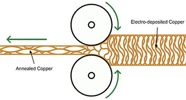
Figure 2. A diagram of how annealed copper is made. (Source: Sierra Circuits)
Since it's never going to be thrown into a landfill, we can get a RoHS exemption to use lead as a plating material. It will be a good old Sn63 eutectic solder. It's the best thing we have for soldering. Ask anyone in the aerospace business. The low-temperature solder process doesn't age the components like the lead-free options could.
Conformal coating or even encapsulating the whole thing in a resin would mitigate the coefficient of thermal expansion differences in the various materials that make up the printed circuit board. I'd like to see the potting material cure and end up like a brick of amber reminiscent of the kind archeologists find with mosquitoes that pestered the dinosaurs.
Exploring capacitor options for the long haul. Meanwhile, those pottery shards stood the test of time, thus the dielectric will go that way as well. Nice thick ceramic to go along with the metal content. It seems like the right material for the capacitors as well, but I worry about cracking. The MLC (multilayer ceramic) caps ought to survive. I'm not sure I even care about size at this point.
Electrolytic capacitors have a good reputation while tantalum caps are overcoming a not-so-good reputation for long-term reliability. Perhaps the mica "jellybean" caps have something to offer. In any case, derating them and distributing the capacitance as much as possible should help.
Resistors are tricky. On a long enough timeline, the expected tolerance increases. The most significant degradation is during bring-up and any other warming events. The immediate aftermath of getting a job is hard on a resistor but it settles in after a while. It could be hundreds of hours for some kinds of resistors though. Quarter-watt axial-leaded resistors with 1% purchased tolerance are going to have to do. We could look at printing some resistors on innerlayers.
Electronics have a habit of either dying young or dying very slowly. None of them is getting out of here without a burn-in to weed out the weakest of the lot. We're going to have to do some serious aging on these. In addition to thermal cycling, we have a salt fog chamber and a shaker table for when we want to do shock and vibe tests. Cycling from hot to cold is one of our best aging processes. Redundancy, derating and overprovisioning are our best fallback plans.
The bathtub curve for the failure rate is the instructive metric. The component engineers will have their hands full testing these things to their breaking points. Screening out early failures is the first pillar of the process. Next comes long-term test-to-failure of those survivors in torture chamber-like environments. All along, we're looking for root causes and designing experiments to single out the most resilient components. Once all the parts are vetted, the process scales up to the board assembly and, finally, the whole piece of equipment.
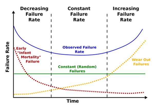
Figure 3. The blue line is a composite of the failure rates attributed to aging of a device. (Source: Wikipedia)
The easy answer to long-lasting products is that getting there must become cultural. An enterprise-wide mindset of continuous improvement is important. Tracking and eliminating defects while documenting both success and failure modes allows us to explore the leading edge while maintaining quality. It's a bad sign when a company shutters the reliability lab. Whatever advantage they may have had is going to fade away.
So, what is this forever-thing we are building? I don't really know. I'm only answering a question posed by a reader. Their name is somewhere in the avalanche of messages that fill my inbox every month. If I'm choosing, it would be something that detects and amplifies faint signals. Whether it is audio or something of a higher frequency, a good analog design stands the test of time.
is a career PCB designer experienced in military, telecom, consumer hardware and, lately, the automotive industry. Originally, he was an RF specialist but is compelled to flip the bit now and then to fill the need for high-speed digital design. He enjoys playing bass and racing bikes when he's not writing about or performing PCB layout. His column is produced by Cadence Design Systems and runs monthly.


Press Releases
- Indium Corporation Experts to Present on High-Temperature, Lead-Free Solder Paste and High Reliability Liquid Metal Alloys Poster at ECTC
- Altus Adds PVA's Game Changing PathMaster X Software to Portfolio
- TRI Opens New Manufacturing Facility
- ROCKA Solutions Set to Rock the SMTA Expos in June with Cutting-Edge SMT Production Supplies!