Solder Defects Causes and Cures Webinar Available
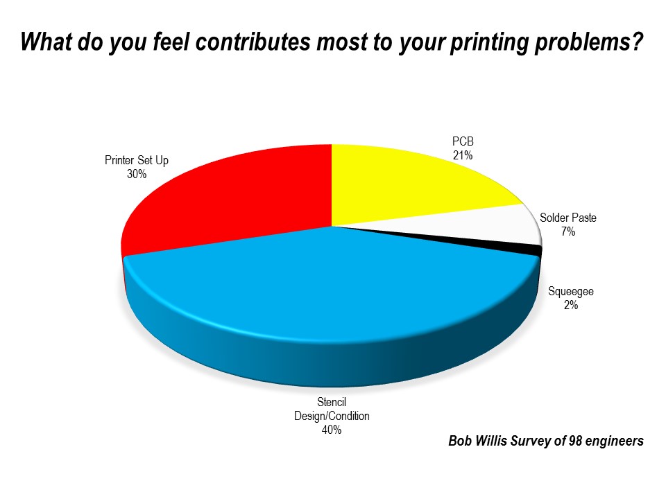
CHICAGO -- A survey of 98 engineers who watched a webinar last week on on solder defect causes and cures found that the majority feel printing is the primary source of defects and stencil design or condition the most likely culprit.
The results were generated by SMT process consultant Bob Willis , whose webinar covers:
- Solder paste inspection standards
- Soldering yield impact with poor printing
- Common solder paste defects
- Impact on reliability based on paste thickness
- Solder joint inspection defects
- Common process defects causes and cures.
Willis is conducting the SMTA-NPL Solder Paste and Solder Joint Automatic Inspection Experience next week at the SMTA International trade show outside Chicago. The event is supported by CIRCUITS ASSEMBLY.
According to Willis, printing solder paste or other conductive material requires zero defects printing if a high first-pass yield is to be achieved when using fine-pitch components. Monitoring and control of paste height and volume are becoming the norm in many markets, but what capability can we expect?
Correct printer setup, good stencil design and manufacture plus consistent printing materials are key to successful manufacture, but inspection and monitoring the performance makes a process more robust. The same three-dimensional inspections are required in other AOI applications like solder joint analysis. There are common process defects during printing and reflow, Willis says, and the webinar shows causes and cures to help yield improvement.