

High-Density Interconnect Technology: An Overview
Design and manufacturing considerations for HDI PCBs.
High-density interconnect (HDI) technology has been a major enabler of advancement in the electronics industry, providing the dense interconnections and intricate circuitry needed to create state-of-the-art electronic devices that are tightly packed with miniaturized components and 2.5-D/3-D semiconductor packages.
Miniaturization at the semiconductor level has driven miniaturization at the PCB level, with manufacturers striving to shrink the size of devices while maintaining or enhancing their capabilities. This has led to the development of compact smartphones, slim laptops, and wearable gadgets that seamlessly blend into our daily lives (Figure 1). Alongside miniaturization has been a constant push for faster processing speeds. As technology evolves, the processing power of electronic devices has skyrocketed, enabling quicker data processing, seamless multitasking, and smoother user experiences.
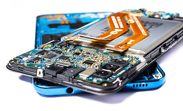
Figure 1. Miniaturization demands for electronics have driven developments at the semiconductor and PCB levels.
Production and assembly of HDI PCBs comes with unique technical challenges centered around reliability and quality. Achieving the intricate high-precision conductive patterns and traces needed to ensure reliability, efficiency and performance requires specialized manufacturing capabilities, particularly where high-layer-count PCBs are required. PCB manufacturers with expertise in HDI technology are helping customers successfully navigate the complexities of designing and fabricating HDI circuitry and enabling the industry to push the boundaries of miniaturization and functionality.
The following provides an overview of standards and best practices for designing and building HDI PCBs.
Guidelines and Standards
Following international guidelines and standards provides manufacturers of HDI PCBs with many advantages. From improved efficiencies and process controls to enhanced product quality and customer satisfaction, adopting international standards as a guide can reduce costs and help gain access to new markets with strict quality requirements.
Among the important IPC and JPCA standards concern HDI PCBs:
- IPC/JPCA-2315, "Design Guide for High Density Interconnects (HDI) and Microvias," which outlines design recommendations for HDI PCBs;
- IPC-2226, an extension of the generic guidelines for PCB design (IPC-2221), which provides in-depth standards and guidance for HDI PCB design;
- IPC/JPCA-4104, "Specification for High Density Interconnect (HDI) and Microvia Materials," which specifies material sets appropriate for HDI PCBs, covering various conductive and dielectric materials that can be used;
- IPC-6012, "Qualification and Performance Specification for Rigid Printed Boards."
These IPC standards collectively provide guidance on HDI PCB design and manufacturing.
2.5-D and 3-D Packaging
Modern semiconductor packaging within the concept of heterogeneous integration plays an important role in miniaturization. Due to challenges of ensuring high yield with larger monolithic silicon processors, heterogeneous integration emerged as a concept for placing multiple diverse semiconductor dies into the same package and connecting them within the package. This essentially consolidates the diverse functionality of two or more components into one smaller package. 2.5-D and 3-D packaging technologies are enabling smaller and more advanced devices through the integration of multiple heterogeneous features and functions into a single component.
2.5-D packaging involves stacking multiple dies or chips on an interposer, which in turn is bonded onto a substrate. 3-D packaging takes miniaturization further by vertically stacking multiple layers of components on a package substrate (Figure 2). These advanced packaging technologies increase functionality while enabling a smaller device footprint. HDI PCB fabrication technology is needed to create the multilayer boards with intricate electrical connection paths that link 2.5-D and 3-D semiconductor packages, and together these technologies have enabled many of the consumer electronics we enjoy today.
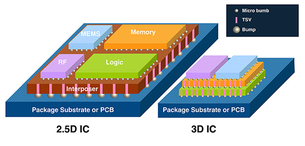
Figure 2. Examples of 2.5-D packaging and 3-D packaging.
Design Considerations
Designing HDI circuit boards necessitates careful consideration of several critical factors to ensure optimal performance, functionality and reliability.
- First and foremost, the layout and placement of components demand meticulous planning to make the most of limited board real estate while preventing signal interference. This includes selecting the right package types and strategically locating critical components.
- Keep track of minimum trace widths and spacing, which can be incredibly narrow, measuring just a few mils (thousandths of an inch) or even less. For example, HDI PCBs commonly feature trace and space widths in the range of 2 mils (50µm) or smaller.
- HDI PCBs use multiple types of vias to make vertical electrical connections. From microvias, and blind and buried vias to stacked and staggered vias, choose via types and placements wisely. Each serves a unique purpose and influences the routing density and signal integrity.
- Pay attention to impedance control, as HDI circuits often handle high-speed signals. Proper impedance matching and controlled trace geometries are crucial to minimize signal reflections and losses.
- Thermal management is another vital consideration, given the higher component density, processing power and speed in HDI boards. Effective heat dissipation strategies, including the use of thermal vias and copper pours, are essential to prevent overheating and ensure long-term reliability.
- Material selection is critical, with consideration of material characteristics such as dielectric constant, thermal properties, and mechanical strength. All materials used to fabricate and assemble the HDI PCB can significantly impact signal performance and board reliability, especially the choice of substrate material.
- Finally, optimize for fewer layers. Boards with higher layer counts require more assembly steps and increase manufacturing costs.
Overall, HDI circuit board design necessitates a comprehensive understanding of the application's specific requirements, precise planning, and a deep knowledge of advanced PCB manufacturing techniques to achieve the desired level of miniaturization, signal integrity and reliability in today's high-performance electronic devices.
Vias Types
All PCBs use layer-to-layer connections, including HDI PCBs. Typical HDI PCBs use more layers than traditional PCBs, however, and require multiple types of vias to create connections between the various layers. From microvias, blind vias, and/or buried vias to via-in-pad, via tenting and plugging, wise selection of via types and their placements requires an understanding of component pin pitches and how electrical signals are designed to flow in the device (Figure 3). This will drive the manufacturing processes used to build the board, as well as the feature sizes placed in the board.
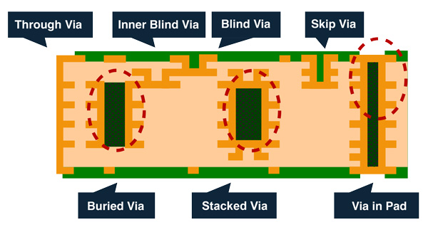
Figure 3. HDI PCBs use multiple types of vias to create connections between various layers.
Through-hole vias (THVs) are the standard via type used to connect different layers in a PCB, including in HDI PCBs. These vias, as their name suggests, traverse the entire thickness of the board, allowing for electrical continuity between top and bottom layers. THVs are well-suited for most applications, including high-power and high-speed designs. They are also preferrable with large components with pin leads such as connectors, where mechanical strength and reliability are paramount.
In addition to THVs, various other via types are used in HDI PCBs, but these other types do not span through the entire layer stackup. Other via types include:
- Blind vias, which connect the outer layers to one or more innerlayers without traversing the entire PCB
- Buried vias, which link innerlayers without extending to the board's surface.
Blind and buried vias are constructed by means of mechanically or laser drilling, depending on the hole diameter required. In general, the smallest mechanical drilling diameter available for use in HDI PCBs is 6 mils. Smaller via diameters must be laser drilled. These smaller vias are called microvias due to their small diameters. In very dense, high layer count boards with many fine-pitch components, microvias may be the only way to route signals in and out of a component.
The advantages of laser drilling are numerous. NC laser drilling provides high precision and fast fabrication, making laser drilling suitable for high-volume production. Laser drilling is also compatible with a wide range of HDI PCB materials, including organic substrates, ceramic-filled PTFE materials and glass-epoxy composites, making laser drilling an ideal choice for diverse PCB applications.
Compared to the smallest mechanical drilling available at 6 mil, the key advantage of laser drilling is faster processing speeds and reduced need for frequent tool replacements. This is what permits laser drilling to be cost-competitive with traditional mechanical drilling. While lasers can provide drilling to varying depths, keep in mind that we are looking for a hole that can be reliably plated. That is why microvias should not exceed a 0.010″ depth with an aspect ratio of 1 to 1 (diameter to depth). Larger ratios and depths will likely result in plating defects. That's why we recommend that laser drilling only be used on thinner HDI buildup layers. Mechanical drilling is better suited for use on thicker layers.
Via-in-Pad
An important design practice in HDI PCBs is via-in-pad, which is the placement of vias directly under surface mount component solder pads, instead of routing the trace around the pad. Via-in-pad serves to miniaturize the PCB size by reducing the amount of space required by trace routing.
Normally, solder would wick through to the back layer of the PCB. To prevent this, via-in-pad requires filling and capping of vias. Filled vias are fabricated by filling traditional through-holes or blind vias with a conductive or nonconductive material. Microvias can also be filled and plated and used as VIP in HDI PCBs.
Conductive filled vias are typically filled with conductive epoxy. The use of conductive materials permits higher current carrying capacity in a PCB. On the other hand, nonconductive filled vias are filled with an insulator that blocks solder flow through the via but does not impact the DC electrical characteristics. To ensure the PCB can be assembled while preventing solder wicking during assembly, filled vias that are used as via-in-pad must also be capped, or plated over with copper. This provides a metal surface where components can be mounted and soldered.
Via Tenting and Plugging
Via tenting and plugging are two processes that involve sealing or covering vias, either partially or completely, to serve various purposes (Figure 4).
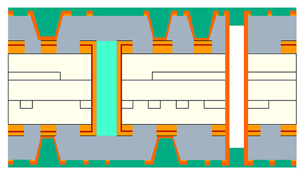
Figure 4. Example diagrams of via tenting and plugging.
Via tenting refers to covering a via with solder mask, whether on one side or both sides. This helps protect against unintended solder bridges or solder wicking occurring during assembly. Tented vias are not to be used with via-in-pad, but they are typically used close to solder pads as an extra precaution against unintended bridging.
On the other hand, via plugging involves filling the via with a nonconductive material to completely seal it (typically without capping). This technique is particularly useful for via protection against environmental factors, such as moisture and dust. Plugged vias will still have an exposed copper ring on the top layer, but solder mask can be used to conceal the leftover copper on the surface.
Direct Metallization
The past decade has seen a notable shift in the preferred method for plating via holes in PCB manufacturing. For many years, electroless copper plating was the dominant approach employed by most PCB manufacturers. This technique involves chemical deposition of a thin layer of conductive copper into the drilled through-holes of multilayer PCBs before electroplating. While the traditional electroless copper process is well established and known for its reliability in creating interconnects, it consumes large amounts of water and energy, uses toxic chemicals and is a significant source of hazardous waste, raising serious environmental and health concerns.
In response to these challenges, innovative electrolytic alternatives to electroless copper plating, often referred to as direct metallization processes, have emerged. Direct metallization involves direct deposition of a thin metal layer onto the inner surface of holes, without the need for prior electroless (chemical) plating. Compared to electroless copper plating, direct metallization provides shorter cycle times, improved hole wall reliability, while dramatically reducing chemical and water usage. Simultaneously, direct metallization processes can reduce costs, energy consumption and carbon footprints.
Direct metallization technologies are transforming the way conductive electrical pathways are fabricated within PCBs and support HDI technologies that produce significantly finer traces with tighter spacing.
For instance, we recently manufactured a 20-layer HDI PCB for a commercial aerospace company. We used a modified semiadditive process (mSAP) as an alternative to subtractive etching to form the conductive circuit patterns. This approach offered better pattern geometry, permitting finer traces and tighter spacing, as narrow as 3 mils (75µm). Having incorporated mSAP helped reduce layer count and cost without compromising signal integrity or reliability.
The market for HDI solutions reflects a continuing opportunity for PCB designers and fabricators. And on the near horizon is ultra HDI (UHDI) PCBs, which are defined as products with conductor widths and spaces of less than 50µm and microvia diameters of less than 75µm.
Those that embrace the trend for smaller, sleeker and more functional devices can position themselves as agile leaders in the HDI (and UHDI) PCB fabrication industry and realize the rewards of participating in groundbreaking innovations while remaining competitive and profitable.
Note: PCEA will sponsor an all-day forum on UHDI & Substrates: Design to Package during PCB East in June in the Boston suburbs.
is chief executive of Rush PCB Inc., a printed circuit design, fabrication and assembly company (rushpcb.com); roy@rushpcb.com.


Press Releases
- SMTXTRA Partners with Quantum Systems to Expand Representation in Key Territories
- KYZEN Announces Exclusive Partnership with Manufacturers’ Representative Restronics Florida
- Koh Young will Showcase its Award-winning Inspection Solutions at SMTconnect with SmartRep in Hall 4A.225 on 11-13 June 2024 in Nuremberg, Germany
- Precision Automation & Assembly Appointed as New England Rep for Kubler US