

5G Open Radio Unit White Box
An overview of the design and development process.
5G radio networks provide increased bandwidth at the expense of reduced range. To compensate for the reduced range and to increase coverage, availability of cost-effective radio units is critical. In collaboration with Intel, Analog Devices, Comcores and Radisys, Whizz Systems has developed a 5G Open Radio Unit (ORU) white box solution to meet this market need. A broader overview of the 5G architecture can be found in Comcores1 and Radisys.2
Here we provide an overview of the design and development process for the various hardware components that make up the 5G ORU white box. Whizz Systems is responsible for the electrical, thermal, mechanical engineering and manufacturing aspects, as well as system validation and bring up of the turnkey white box ORU solution. This includes design of the individual PCBAs and industrial design of the enclosure.
The hardware design leverages Intel's Arria 10 reference design as a starting point, with power and clocking schemes revamped to meet the updated power and clocking requirements for the ORU platform. An additional JESD interface as a communication pathway is added between the Arria 10 FPGA and Analog Devices-based chip ADRV902X. A board-to-board (BTB) header is added to mate with either the ADI-designed radio frequency front-end (RFFE) card or the Whizz-designed ORU adapter card.
SI/PI simulations are carried out to guarantee the design meets requirements of the 5G ORU. The mechanical team designed the chassis and simulation of thermal characteristics of the board for heat sink and fan selection.
The 5G white box PCB is fabricated at Whizz Systems using internal standards for process and inspection. The manufactured board is tested for shorts, proper power on sequence, and bring up of all interfaces. Finally, the software team is involved for validation of QSFP, DDR, Madura and other major subsystems.
Hardware Electrical Specifications
The white box product consists of both the ORU PCBA and the RFFE PCBA, but the focus here is mainly on ORU design. The ORU card is designed using a low-power, high-performance and logic-intensive Arria 10 SoC processor to create custom radio solutions with 4T4R TDD (four transmit and four receive time division duplex) communication radio link with a tunable range of 600MHz to 6GHz, with a 100MHz signal bandwidth (oBW).
The white box ORU card design supports Arria 10 SX 320/480 SoCs and has onboard 1GB DDR4 HPS memory and 2GB DDR4 FPGA memory (Figure 1). The design also hosts a 1Gbps Ethernet interface, a USB-to-UART interface, and two optical QSFP ports with each channel capable of 10Gbps, with a total transfer rate of 40Gbps along with 1PPS/10MHz clock for external synchronization. Two warm/cold reset push switches for the Arria 10 are on the faceplate along with a slide switch for power cutoff.
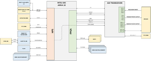
Figure 1. System block diagram for the ORU card.
The Arria 10 communicates with the QSFP ports using two SERDES banks, has dedicated RGMII interfaces for the ethernet port, and uses a UART port for UART-to-USB conversion. HPS/FPGA banks are used for the HPS/FPGA memories whereas a JESD interface in the form of SERDES is used to communicate with the ADI ADRV902X chip.
The user can use the onboard BTB boot flash connector to mount either an SD card module or a QSPI module as boot-up options for the device. The board also hosts a total of three fan headers, eight user LEDs, an eight-port SPST dip-switch and six-pin user IO connector.
The 5G white box radio card also provides support for IJ5 series Samtec board-to-board connector for an external RFFE/adapter board and another board-to-board connector for an external SD card boot flash for the Arria 10 SoC. Figure 2 shows various components of the ORU PCBA.
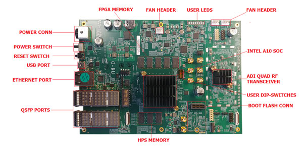
Figure 2. ORU PCBA.
PCB Layout
PCB layout is performed with consideration for electrical and mechanical constraints for the application of the unit. The dielectric material is Isola 408HR, chosen because it's cost-effective and simulation/lab results of insertion loss are low enough for the required maximum signal speed.
Several layout techniques are used for improved performance. For example, backdrilling is adopted to eliminate stubs, and separate analog/digital sections are employed to reduce noise and interference. Moreover, standard through-hole via technology is used to reduce cost.
Reference planes are taken into consideration while routing high-speed signal pairs. Fewer bends and optimized trace lengths are achieved to minimize signal losses, maintaining adequate space within traces and to all other features. Electrical rules checks (ERC) and design rules checks (DRC) are run to ensure all established constraints are met.
Layout iterations are made based on analysis feedback such as thermal simulation, enforced placement of power supplies and mechanical allowance for heat sinks. Connector placements and enclosure-related changes are driven by 3-D modeling of all subsystems. SI/PI simulation recommendations are implemented for verification of optimum board functionality. Figure 3 shows the RFFE and ORU cards.
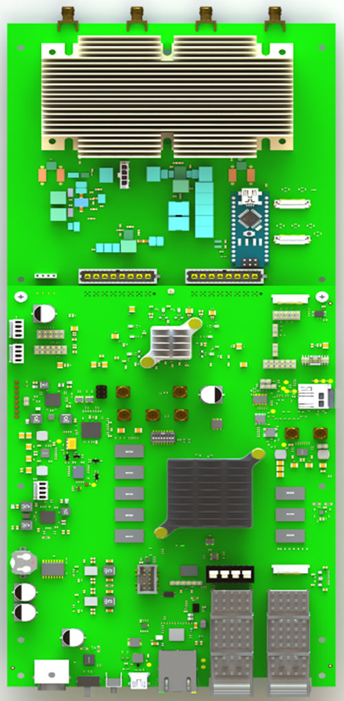
Figure 3. RFFE and ORU cards.
Among the challenges involved are making a special GND shield around ADI chip for RF signal isolation, FFC connector placement due to its connecting cable length constraint, power supply layout design due to complex copper pour shapes, implementation of special GSSG via pattern, and plane voids for high-speed signal integrity of QSFP signals.
SI/PI Simulations
Multiple simulations are run to optimize functionality and performance of each interface, minimizing chances of design revision.
Stackup is calculated by selecting the dielectric material type required to meet the signaling performance requirements. Prepreg/copper thickness as well as the number of signal layers/GND/power planes are carefully set up to meet the design requirements and maintain cost-effectiveness. Trace width calculations are performed to meet impedance requirements.
Parametric via optimization simulation is also performed to design an impedance-controlled via for minimizing signal losses (Figure 4).
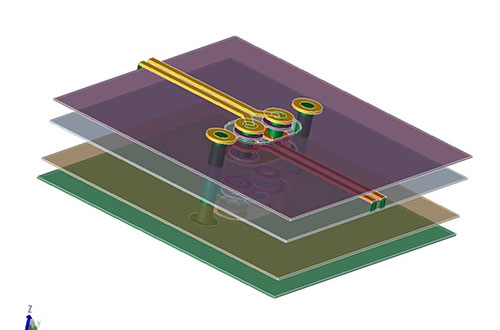
Figure 4. 3-D via structure for design optimization.
Critical high-speed signal design rules like maximum allowed trace length are defined through several pre-layout simulations. This is the key to first time success of this design. The via stub is minimized by back-drilling to reduce return loss and improve signal quality of the high-speed differential pairs (Figure 5). To validate the routing rules, insertion and return loss measurements as well as serial link simulations are performed for the QSFP signals which produce eye diagrams (Figure 6).
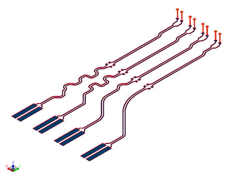
Figure 5. 3-D view of high-speed routing.
The DDR interface is demanding in terms of signal integrity and timing requirements. To ensure the DDR interface functions properly, pre-layout simulations are run to determine routing topology and set delay matching rules. The termination resistor value selected minimizes ringing, noise and reflection. Post-layout simulation is done to get eye, wave and timing/mask results for verification that the signals are matched within required timing with less ringing and maximum eye-aperture widths.
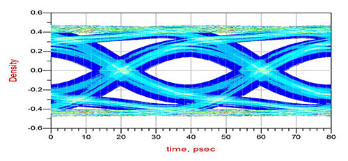
Figure 6. Eye diagram results of serial link simulation.
Power is one of the main challenges faced in designing this board. Power AC simulation is done to optimize the power delivery network and reduce the cost of decoupling/bypass capacitors.
Power DC simulation is run to ensure that the IR drop is within acceptable limits for this design. Care is taken while selecting ferrite beads, inductor or supply regulators for critical power rails to minimize IR drop and thermal heating issues. To ensure the PDN circuit will work effectively, IR drop, via current, plane current density, and Joule heat thermal simulations are performed on all power rails. Figure 7 shows IR drop simulation results.
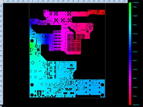
Figure 7. Power DC analysis results.
Mechanical Enclosure
The mechanical board and enclosure size are designed optimally to meet the overall product design constraints and requirements. The ORU card size is 9 x 6 x 1.5″; the adapter card is 6.5 x 6 x 0.5″ and the RFFE card is 6.4 x 6 x 1.2″. The overall enclosure size specifications are 14.9 x 8 x 2.6″ (Figure 8).
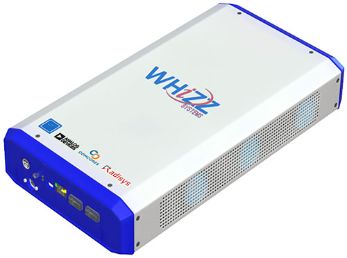
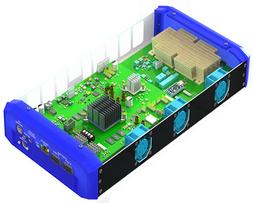
Figure 8. ORU enclosure.
Sheet metal for the enclosure is aluminum alloy, which is lighter and easier to manufacture compared to options such as low-carbon steel. Encapsulations are ABS plastic, which is inexpensive, lightweight, shock-absorbent, and durable.
Off-the-shelf hardware selection is generally preferred for mechanical assembly for lower cost and simplification. This includes washers, screws, standoffs, and other mechanical components.
Several enclosure joining mechanisms like sliding, top/bottom joining, etc., are used, but mating of covers with screws is preferred, in consideration of the application of the unit. Chassis shape design underwent several revisions for contour changes to lower the cost while retaining aesthetic appeal.
Thermal Analysis
ORU and RFFE cards are thermally simulated to determine critical components temperature and heat flow under certain power loads and ambient conditions. The objective is the critical component temperatures must not exceed the rated maximum temperature range.
The unit is thermal compliant for system-level (inside the enclosure) as well as module-level (the standalone PCB), verified using a CTM (compact thermal model).
Different configurations are applied for both the ORU and RFEE cards. Connectors and heighted components in the ORU are positioned to ensure no airflow blockers, and that temperatures are within the allowed range. Heat sinks are selected according to major heat-dissipated components. As the RFFE is designed after ORU, configurations for the RFFE are optimized for a new fan with more airflow but the same position.
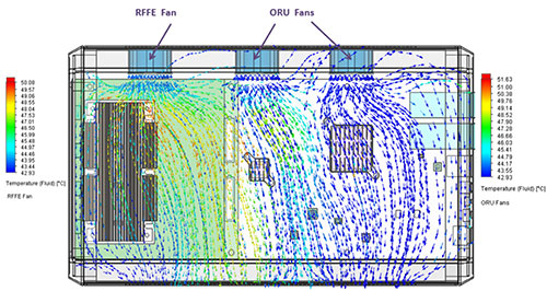
Figure 9. Thermal analysis results.
As a result, all thermal model simulation results are PASS based on selected thermal solutions of heat sinks and fans with better air flow but less pressure noise (Figure 9).
References
1. Comcores, Part 2: Opening the 5G Radio Interface, Design & Reuse,
https://www.design-reuse.com/articles/48289/opening-the-5g-radio-interface.html.
2. Radisys, Delivering an Open Radio Unit for Outdoor Small Cell Deployment, company white paper, https://hub.radisys.com/white-papers/delivering-open-radio-unit-for-outdoor-small-cell-deployment.
is founder and CEO at Whizz Systems; mirfan@whizzsystems.com.


Press Releases
- SMTXTRA Partners with Quantum Systems to Expand Representation in Key Territories
- KYZEN Announces Exclusive Partnership with Manufacturers’ Representative Restronics Florida
- Koh Young will Showcase its Award-winning Inspection Solutions at SMTconnect with SmartRep in Hall 4A.225 on 11-13 June 2024 in Nuremberg, Germany
- Precision Automation & Assembly Appointed as New England Rep for Kubler US