

Selectively Assembling High-Value Components Based on Warpage in Order to Improve Reliability
Can predicting board and part flatness at critical points in the reflow/reliability profile reduce failures?
Surface warpage, or flatness, is an established source of reliability issues in surface mount devices (SMD), particularly when these surfaces are considered as they warp due to heat generated in production or real-world use.1-6 Thermal warpage of surface mount components such as ball grid arrays (BGA) and line grid arrays (LGA) are subject to different industry standards from JEDEC, JEITA, and IPC, based on sample size, ball size and ball pitch.7-9 Further SMD studies have proposed different methods of classifying and qualifying surface shape in hopes to improve the correlation in thermal warpage data and product reliability.10 Meanwhile, printed circuit boards are less regulated for warpage in the area where an SMD may attach. Overall PCB warpage is referenced in some industry standards and technical papers, but specific warpage limits are lacking within documentation discussing warpage of SMD landing areas.11-12 Finally, further studies have considered warpage of both SMD and PCB landing areas together.13-14
The approach of considering the shape of both sides of a surface mount interface is used as the basis for this study. To fully understand warpage gaps that create defects, both sides of the attaching interface are required. The trend for larger BGA packages in high-speed network applications is furthering the need for managing warpage on both the SMD and PCB sides of the assembly.15 Larger package footprints permit more lateral space in which shape change can occur due to either starting sample shape or thermal warpage.
While measuring samples for thermal warpage is a common practice, this study is proposing a much different approach to improve product reliability. This study presents a concept of measuring warpage on 100% of high-value SMD devices and 100% of the PCB landing areas where they would attach in assembly, then deciding which sample to place on which PCB. This study is very much a first step and does not provide a final approach or hardware configuration to accomplish such a quality control approach. Matching initial surface shape alone to minimize initial gaps between BGA and PCB landing sites may also be a value add and simpler approach. However, gaps at high temperature points in the reflow profile are more problematic for creation of surface mount defects.16 Therefore, this study focuses on the ability to predict what shape will be during reflow, based on a sampling of thermal warpage data and 100% measurement of room temperature shape. Thermal warpage testing is often considered destructive, thus cannot be used for 100% inspection in production.
Experimental Methodology
Warpage metrology approach. Shadow moiré and digital fringe projection (DFP) warpage measurement techniques are discussed in this study. Both are referenced in industry standards related to warpage, though DFP is excluded from JEITA standards on package warpage.7-10 Shadow moiré is exclusively used for the data of this study, focused on accurate thermal warpage behavior of SMDs and PCB local areas. This technique is best used for continuous surfaces and provides a highly accurate approach whose accuracy does not scale with larger areas of measurement.17 Although shadow moiré may be viable for the production room temperature measurements, here DFP is hypothesized to be the preferred approach for 100% room temperature measurements, being the more portable of the two techniques.
Shadow moiré measures surface shape by shining a line light through a Ronchi rule grating, a piece of glass with alternating clear and opaque lines, having a common pitch from 50-500µm. This creates a contour map via an interference pattern generated between the lines and the shadow cast by the same lines. A phase-stepping technique is also applied for increased resolution. FIGURE 1 shows the shadow moiré concept, and FIGURE 2 shows a created contour pattern.
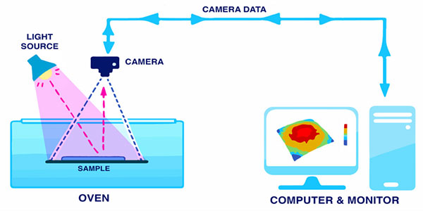
Figure 1. Shadow moiré visual concept.
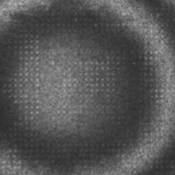
Figure 2. Shadow moiré pattern.
DFP also measures surface shape and uses a phase stepping approach to improve resolution. Calibration is achieved by measuring an optical flat at different heights. Here a pattern is projected instead of an interference pattern created. The calibration flat and measured sample are compared to show surface shape. Fringe density can be varied as well as shifted, limited by the projector resolution only. Varying fringe pitch helps in measuring sudden sample height changes. FIGURE 3 shows the DFP technique and FIGURE 4 shows a surface with fringes projected on dome like contours on an overall flat surface.
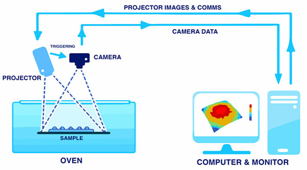
Figure 3. Digital fringe projection visual concept.
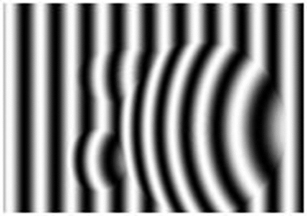
Figure 4. Digital fringe projection pattern.
Test samples. For the purposes of intellectual property protection, sample descriptions and details are left generic in this study. Here only a conceptual approach is presented and not details on specific samples and their warpage behavior. The purpose of testing these samples is to show how thermal warpage can be correlated to initial room temperature shape for the purposes of predicting surface mount defects. This also addresses the specific functions, such as matrix subtraction and averaging, to implement such as approach.
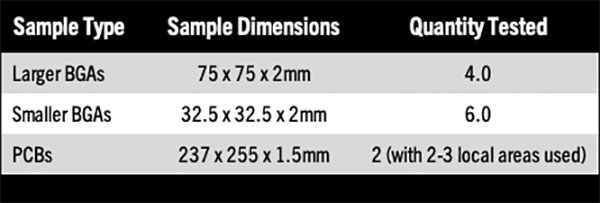
Multiple samples of two package types are measured for warpage across reflow temperatures. Additionally, a couple of PCBs are measured for warpage. Local areas sized to match the footprint of the package sizes will be used for comparison of warpage between package and PCB area. Details of the test samples and quantities are shown in TABLE 1.
Table 1. Test Samples
Test setup. Samples were prebaked 24 hrs. at 125°C to reduce possible effects on warpage from moisture in the samples.18 Oven settings were optimized around sample temperature uniformity, per standard operating procedures. All samples were subject to the same thermal profile, shown in FIGURE 5.
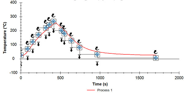
Figure 5. Thermal profile output.
Smaller package samples were supported on Robax glass with controlling thermocouple attached to the top surface of a dummy sample for testing. The larger package samples were supported by metal rails along the horizontal edges with a controlling thermocouple on the bottom surface. There were test setup samples with both top and bottom surface thermocouples run with the thermal profile used in all subsequent tests to optimize the oven time and temperature settings to ensure a top/bottom uniformity of +/-5°C or less. PCBs were tested on metal rails held from the edges with thermocouple attachment to the bottom surface. All other test setup variables were kept the same between sample measurements. Example setups of the package and PCB samples are shown in FIGURE 6 and FIGURE 7.
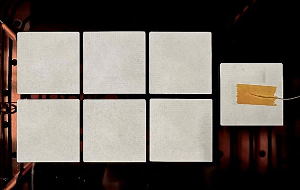
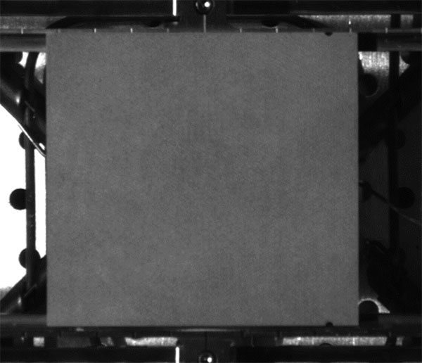
Figure 6. Package samples (Top: smaller BGAs; Bottom: larger BGAs) test setup in oven.
Figure 7. PCB sample test setup in oven (blurred to protect manufacturer).
Shape matching. Here only two PCBs are tested. Different local areas from the PCB are digitally extracted to match the specific size of the BGA land area. For the smaller BGA, three local areas are chosen around the PCB, thus two PCBs and three local areas are compared across temperature to the six smaller BGA samples. Similarly, two local areas are chosen with physical size matching the larger BGA, thus four regions of comparison are created across temperature. Note that the BGAs and PCBs are not specifically units that are assembled together in a real-world production scenario.
Offset methods and gauge choices to quantify 3-D shape are another critical decision. In this study, closest point touching is exclusively used as the offset method. This addresses how top and bottom surfaces are combined together for comparison. With all offset methods, sample Pin 1 location and measured surface, inner or outer, are tracked in sample metadata for use in software comparisons. For gauges, maximum gap will be the data focus. Other gauges such as average gap and compatibility, however, could be useful gauges to consider. These gauges are defined as follows:
- Closest point touching: offset method – The top and bottom surfaces are brought together with their LSF (least squares fit) planes parallel until the first point touches.
- Maximum gap: The maximum distance between the top and bottom surface out-of-plane.
- Average gap: The average distance between the top and bottom surface out-of-plane.
- Compatibility: The RMS (root mean square) deviation between the top and bottom surface out-of-plane.
Room temperature interface analysis. The most basic iteration of using shape matching to decide mating surfaces is purely to consider both shapes at room temperature only. In FIGURE 8, artificially created surfaces are used to demonstrate the concept.
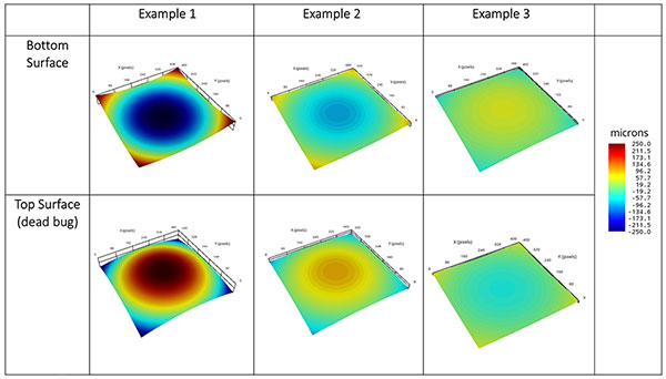
Figure 8. Surface matching example.
In Figure 8, flipping top surface 1 onto bottom surface 1 as they would be assembled creates a surface with no gap, a fully flat plane. The same is true for examples 2 and 3. However, assembling top surface 3 onto bottom surface 1 would create a surface with significant shape between the mating surfaces (FIGURE 9).
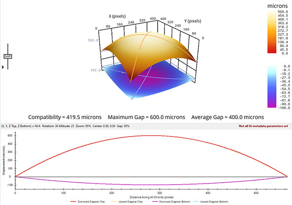
Figure 9. Interface analysis of poorly matched mating surfaces.
Figure 9 shows the potential importance of selectivity in which samples to mate. In a real-world scenario, the differences between samples are unlikely to be this extreme, but studies have shown that sample variation even at room temperature can affect product yield.19
Prediction of relative shape change in thermal warpage. While matching surfaces based on room temperature shape is a possible approach to improve yield, here the argument is made that a prediction of what surface shapes will be at a critical point during reflow is the more valuable data point. The area around solder liquidus is of particular interest for good solder joints. It is hypothesized here that a collection of thermal warpage data can be used to predict the relative shape change of a surface over temperature. To create this data set, relative shape change from room temperature to solder liquidus is rendered. These surface matrices are then averaged together to predict the relative shape change of the sample using only room temperature data. Examples of this process are shown in actual measurement results.
Results
Data were taken through a full reflow profile as shown in Figure 5. However, only room temperature shape and shape at 220°C on the cooling side of the profile is analyzed in this study. Warpage result gauges are presented in microns throughout.
Room temperature interface analysis. TABLE 2 shows the maximum gap in microns at room temperature of the six smaller BGAs interfaced with PCB1 and two at all three ROI (regions of interest), considering every possible combination. FIGURE 10 shows one example interface graphically.
Table 2. Room Temperature Maximum Gap of all Interface Combinations, Smaller BGA
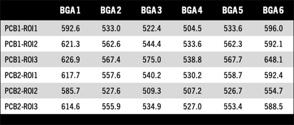
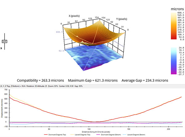
Figure 10. Room temperature interface analysis between smaller BGA 1 and PCB 1 – ROI 2.
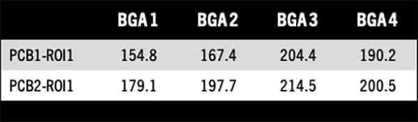
TABLE 3 shows the maximum gap in microns at room temperature of the four larger BGAs interfaced with PCB1 and PCB2 at ROI 2, considering every possible combination. FIGURE 11 shows one example interface graphically.
Table 3. Room Temperature Maximum Gap of all Interface Combinations, Larger BGA
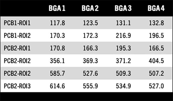
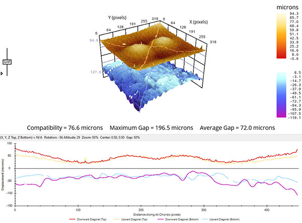
Figure 11. Room temperature interface analysis between larger BGA 4 and PCB 1 – ROI 2.
Interface analysis at actual solder liquidus. Since we have thermal data for all samples, here we analyze interface gaps at a solder liquidus of 220°C on the cooling side of the profile. Later this shape will be predicted using an average of relative shape change from room temperature to 220°C. TABLE 4 shows the maximum gap in microns at 220°C of the six smaller BGAs interfaced with PCB1 and 2 at all three ROI, considering every possible combination. FIGURE 12 shows one example interface graphically.
Table 4. Solder Liquidus (220°C) Maximum Gap of all Interface Combinations, Smaller BGA
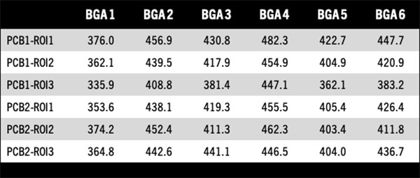
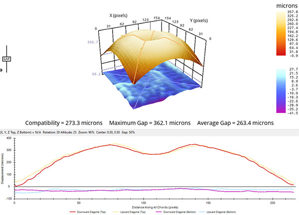
Figure 12. Solder liquidus (220°C) interface analysis between smaller BGA 1 and PCB 1 – ROI 2.
TABLE 5 shows the maximum gap in microns at solder liquidus of 220°C of the four larger BGAs interfaced with PCB1 and PCB2 at ROI 2, considering every possible combination. FIGURE 13 shows one example interface graphically.
Table 5. Solder Liquidus (220°C) Maximum Gap of all Interface Combinations, Larger BGA
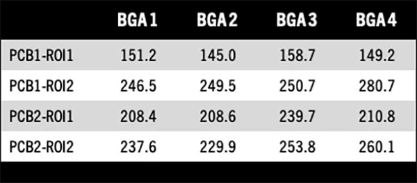
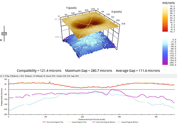
Figure 13. Solder liquidus (220°C) interface analysis between larger BGA 4 and PCB 1 – ROI 2.
Relative shape change room temperature to solder liquidus. For each measured surface, the relative shape change between room temperature and 220°C can be found by subtracting the room temperature surface from the 220°C surface as in FIGURE 14.
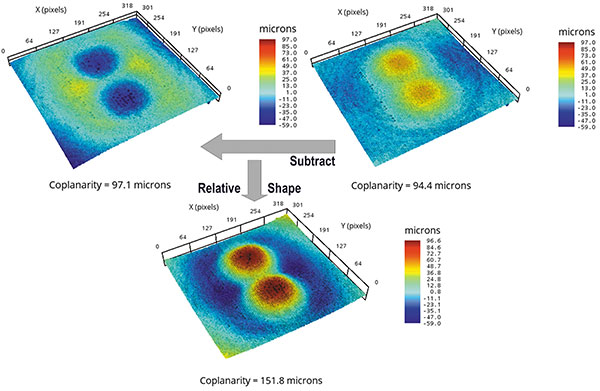
Figure 14. Relative shape change in BGA 4 from room temperature to 220°C.
This process is repeated for all surface data. Then relative surfaces for each ROI are averaged together. FIGURE 15 shows the four average relative warpage change surfaces for the PCB and BGA in larger and smaller sizes between 220°C and room temperature.
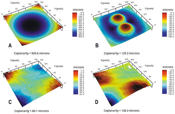
Figure 15. Average relative shape change from room temperature to 220°C; a) smaller BGA, b) larger BGA, c) smaller PCB all ROI, d) larger PCB all ROI.
Prediction of shape at solder liquidus based on average shape change. The final step is to use these averaged surfaces, applying the shape change to the room temperature surface to try and predict what the shape will be at the critical solder liquidus point in the reflow profile. The example from Figure 14 can be used again in FIGURE 16. The average relative shape change is inverted and then subtracted from room temperature data to predict the solder liquidus shape.
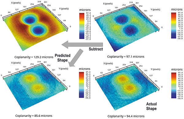
Figure 16. Predicted larger BGA shape at 220°C based on room temperature shape and average relative shape change.
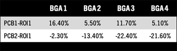
This same process can be repeated for all surface to recreate max gap numbers using the relative shape change prediction and actual room temperature shape of both PCB and BGA surfaces. The hope is to find similar numbers found in Tables 4 and 5. Given the highly different shape changes of the multiple PCB regions, only ROI 1 from the PCB data is used in this process. The overall concept of this predictive method is that shape change over temperature is somewhat repeatable for samples of equal design and production conditions. TABLES 6 and 7 show the results from the transformed room temperature data.
Table 6. Predicted Maximum Gap at Solder Liquidus of Interface Combinations, Smaller BGA
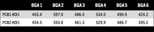
Table 7. Predicted Maximum Gap at Solder Liquidus of Interface Combinations, Larger BGA
Discussion
Shape prediction accuracy. Further data analysis starts with qualifying the accuracy of the predictive approach in using average relative change over temperature to predict sample shape at temperature. TABLES 8 and 9 show the percentage error of actual maximum gap between interfaces at 220°C and the predicted gap.
Table 8. Prediction Error of Maximum Gap at Solder Liquidus of Interface Combinations, Smaller BGA
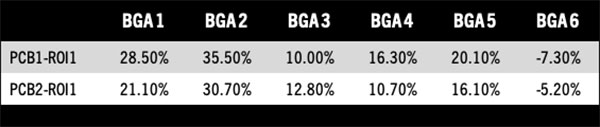
Table 9. Prediction Error of Maximum Gap at Solder Liquidus of Interface Combinations, Larger BGA
The error in the prediction is significant. This could be attributed to the age and unknown history of the samples used, however. The PCBs and small BGA were both older products with unknown thermal history. Realistic samples of the application may see different results under this presented model. Notably, the larger BGA was the more realistic and more modern package used in the study, and it showed more consistent change under reflow temperatures. While the error was significant in Table 9, predictions are consistently high for PCB1 and low for PCB2, suggesting variation in the PCB could be the larger inconsistency. Larger data sets may also aid in establishing a baseline relative thermal warpage change.
Practical production implementation. The approach proposed in this study assumes a percentage of destructive thermal warpage testing on samples in question. This is an industry practice used by many companies, with referenced standards.7-9,11 It also assumes 100% flatness inspection of both bare PCB surface mount attach areas, however, as well as flatness measurement of designated high-value components. Flatness inspection of these items is not standard industry practice.
Physical space and methodology to take these measurements must be considered. PCBs would need to be measured prior to solder paste application. Measuring components within tape-and-reel is likely unrealistic. But, many high-value components will be presented to pick-and-place machinery in JEDEC trays, making automated flatness inspection during assembly more viable. Components in JEDEC trays would also typically be sitting live bug, such that the topside is visible for measurement instead of the attach side. Industry standards for thermal warpage instruct measurement of the attach side, but they also include removal of solder balls when present, which is not practical for production, given the destructive nature.7-8 Therefore, correlation of the shape on top of the sample may be needed, unless further complexity is added to inspect the attach side of the component. Even in this case, BGA components have the challenge of measuring substrate surfaces between the solder balls, which presents some metrology challenges for more densely populated components. With the availability of optical metrology techniques, measuring sample shapes can be done at high speeds relative to typical reflow production processes and are not expected to increase production times.
Communication with pick-and-place machinery would be required to implement such a solution. The level of communication required would be highly simple, however, only needing to indicate which samples should be picked up next. Additionally, possible physical integration between pick-and-place tools and JEDEC loading mechanisms may be required. Measuring samples as they are loaded into the pick-and-place tool would be a likely place to capture component shape, possibly taking multiple measurements per tray to improve measurement resolution, versus requiring motion systems for the metrology optics or multiple optical hardware setups.
The quantity of available data upon which to make decisions would depend on the timing of the assembly process. The discussed examples assume that a handful of data are available at the same time to place combinations of samples together. The criteria for making this decision could be numerous, including many different types of gauges, including the referenced average gap and compatibility gauges. This could potentially also include a level of criteria that would fail inspection and be removed from the assembly process. A failure level is not required for the approach.
The portability of the DFP technique may be a better fit for a production scenario. Studies have shown that DFP and shadow moiré techniques can be correlated with appropriate control of variables.17 Thus, the shadow moiré technique could be used for thermal warpage data and establishing average relative change data, even if DFP is used for production flatness measurements.
Conclusions
A potential approach to improve yield in the reflow assembly process is presented. The approach and data presented here are only a first phase concept, rather than a fully established solution for implementation. Further studies, using more realistic mating samples, is the recommended next step. Further steps include establishing conditions for acceptable interface gaps, further studying product warpage and production yield, communications with production equipment, and creation of production tools for warpage measurement of samples at room temperature.
Error in the prediction scheme is significant. The error here may come down with more realistic samples and larger product samplings. While the error is significant, the study also shows that the gaps between the samples at room temperature and at critical solder liquidus temperatures are noticeably different. Thus, using room temperature shape differences alone is not expected to provide the necessary information for selectively assembling component to board.
Strong control of product history and realistic reflow emulation in thermal warpage metrology will be essential to enable prediction of surface shapes at critical points in the reflow process.
Acknowledgments
The authors would like to thank Ryan Curry of Akrometrix for applications guidance and support.
This article is adapted from a presentation at the 2023 IPC Apex Expo Technical Conference and is published with permission of the authors.
REFERENCES
1. W. Loh, et al, “Recent Trends of Package Warpage Characteristic,” International Conference on Electronics Packaging (ICEP), 2015.
2. K. Peng, et al, “Reflow Warpage Induced Interconnect Gaps between Package/PCB and PoP Top/Bottom Packages,” Proceedings of ECTC, 2017.
3. A. Mawer, et al, “Effect of Package Warpage and Composite CTE on Failure Modes in Board-Level Thermal Cycling,” Proceedings of SMTA International, 2018.
4. J. Kim, et al, “Warpage Issues and Assembly Challenges Using Coreless Package Substrate,” Proceedings of IPC Apex, 2012.
5. K. Ishibashi, “PoP (Package-on-Package) Stacking Yield Loss Study,” Proceedings of IPC Apex, 2012.
6. R. Darveaux, et al, “Reliability of Plastic Ball Grid Array Assembly,” Ball Grid Array Technology, J. Lau Editor, McGraw-Hill, 1995.
7. JEDEC Solid State Technology Association, JESD22-B112B, “Package Warpage Measurement of Surface-Mount Integrated Circuits at Elevated Temperature,” August 2018.
8. Japan Electronics and Information Technology Association, JEITA ED-7306, “Measurement Methods of Package Warpage at Elevated Temperature and the Maximum Permissible Warpage,” March 2007.
9. IPC, IPC-7095D, “Design and Assembly Process Implementation for Ball Grid Arrays (BGAs)” June 2018.
10. N. Hubble, et al, “Surface Mount Signed Warpage Case Study; New Methods for Characterizing 3D Shapes Through Reflow Temperatures,” Proceedings of IPC Apex Expo, 2017.
11. IPC, IPC-9641, “High Temperature Printed Board Flatness Guideline,” June 2013.
12. J. Davignon, “PCB Dynamic Coplanarity at Elevated Temperatures”, Proceedings SMTA International, 2011.
13. J. Arellano, et al, “Thermal Shadow Moiré to Cross-Section Correlation Study,” Proceedings of SMTA International 2018.
14. K. Chiavone, “Advanced Second Level Assembly Analysis Techniques – Troubleshooting Head-In-Pillow, Opens, and Shorts with Dual Full-Field 3D Surface Warpage Data Sets,” Proceedings IPC Apex Expo, 2013.
15. J. Savic, “Warpage Mitigation Processes in the Assembly of Large Body Size Mixed Pitch BGA Coreless Packages for Use in High Speed Network Applications,” Proceedings of SMTA International, 2013.
16. Z. Zhao, et al, “Effects of Package Warpage on Head-in-Pillow Defects,” Materials Transactions, vol. 56, Nov. 2015.
17. N. Hubble and L. Weaver, “Comparing Shadow Moiré and Digital Fringe Projection Warpage Metrology Techniques,” Proceedings of SMTA International, 2017.
18. N. Hubble, “High Temperature Component Warpage as a Function of Moisture Sensitivity (MSL) Rating,” Proceedings of SMTA International, 2019.
19. D. Adams, et al, “Understanding PCB Design Variables that Contribute to Warpage During Module-Carrier Attachment,” Proceedings of SMTA International, 2016.
is president and is an electrical engineer at AkroMetrix (nhubble@akrometrix.com).


