Managing Printed Circuit Board Designers
 Schedules are not the only thing to prioritize.
Being a manager isn’t for everyone. In addition to technical skills, a manager is responsible for resource allocation and risk management. In the field of electronic design, a manager must balance being a technical person and a people-person. Beyond that, a manager overseeing employees involved in creative endeavors must comprehend the uncertainties and challenges that arise with an electronics design project. Of course, the electrical engineer will normally say the schematic is complete on the day it is supposed to be. Same goes for the mechanical engineer. Ever the optimists, they believe everything is going according to plan – until the day it isn’t. Surprise! (Though, honestly, it’s not really surprising.)
What makes PCB design work different? One of the interesting things about printed circuit design is that no two boards are exactly alike. Every day is something new. That alone makes it hard to quantify the work involved with a new project. While some aspects can be seen as repeatable, the details always differ.
A key factor for scheduling is the number of pins in a circuit and the amount of space allocated for each pin. These two figures can serve as a metric for estimating the expected duration of the design cycle, as well as providing insight into the layer count and other physical dimensions. There is, however, a more nuanced variable to consider: the nature of the devices involved.
Analog signals or high voltage requirements will eat up more real estate than an equal number of digital signals. The exception here is memory, especially DDR devices which require more space and time for the intensive length matching involved. Any device that is described as a sensor will likely require special handling.
Any of these features likely requires simulation for signal and/or power integrity. This process often isn’t a one-and-done effort but an iterative one. When a designer sees something for the first time, it will likely take longer to complete. Designers usually need to digest data sheets and app notes along with the netlist. I believe this requirement contributes to the detailed job descriptions for designers, specifying the types of circuit design experience needed.

Figure 1. A good chair is almost as important as a large screen. The designer incorporates data sheets and app notes with schematic and the power tree, along with email and other micro-communications. This is in addition to the actual layout where the more we can see, the more we can do. (Source: Author)
Hiring the right designer. The company cannot afford to blunder its way through a design program through trial and error. What we see as a result is a great demand for senior PCB designers with specific skillsets. The aspiring applicant needs to use the institutionalized ECAD software while doing work that has direct parallels to what the hiring manager requires. A startup will have fewer resources than a multinational enterprise.
That disparity can mean that the startup will want someone who can pivot over to the test bench and help troubleshoot the boards once it gets to that stage. That requirement will exclude designers who are not hands-on when it comes to using a soldering iron or multimeter.
The hiring manager in a startup will face challenges in finding and recruiting qualified employees. This challenge remains true even when they are not searching for a designer/technician. Most board designers prefer companies with more perks, including job security and, in many cases, name recognition. Bigger companies hold an advantage in that regard.
Small companies provide opportunities for individuals to excel without the rigid reporting structure. Like a small town where everyone knows everyone, employees can cut through the red tape and get things done. They have the chance to change the world with their agility. Employees from the early days have the “tribal knowledge” and the chance to grow with the company. They are usually in position to include a higher amount of company ownership along with monetary compensation. Use these advantages as part of the incentive to join the “underdog.”
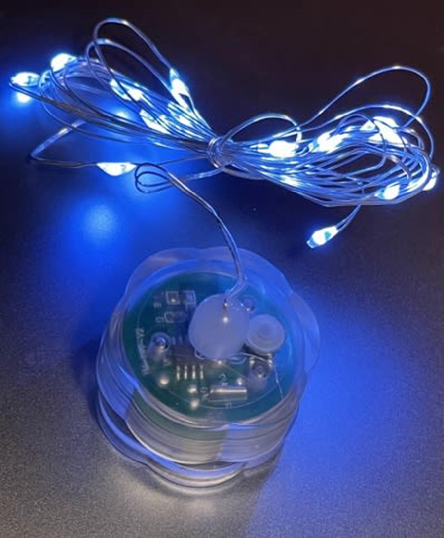
Figure 2. A small, printed circuit board can still go sideways if there are factors that are not known to the designer. (Source: Author)
The schedule is most important but far from the only thing. Stressing schedules over everything leads to shortcuts which can end up backfiring. I had a manager who took it the other direction. Yes, we needed to finish the work, but the overarching goal was to have no questions from the vendor(s) once the design package went out for fabrication and assembly. Give me a four-layer board with no controlled impedance and I can do that.
Once we’re using sequential lamination and specific linewidths for various purposes, the chances of clearing the DfM and DfA cycles without a technical question would evaporate. Even starting with a vendor-supplied stack-up and trace geometry was no guarantee the vendor wouldn’t have a new “and improved” stack-up created to clear out some raw inventory at the shop.
Sending the board for quotes at multiple fabricators is a sure way to get conflicting DfM reports. Using high-density interconnect (HDI) or ultra-HDI is another way to have the vendor try to stall the start date. I’m not speculating that the vendor does that simply to buy more time: I’ve heard them say as much in a moment of candor. I share this to provide an understanding in how the game is played on the leading edge.
DfM defects come in different flavors. A vendor utilizes a method for checking boards that features three tiers of technical questions. A red error indicates an issue they cannot resolve. Orange errors flag problems that can be addressed but will yield lower production quality. Eventually, yellow errors would show up for nice-to-have corrections In the first iteration, the team must eliminate red errors while allowing orange and yellow errors to pass through. In the next revision, they will prioritize addressing mid-tier orange defects flagged for design for manufacturability (DfM).
As time progresses, they will continually identify minor details that can be improved. The vendor isn’t about to disclose this stuff upfront; however, the issues acceptable in the first iteration may only scratch the surface of potential design improvements. Steady incremental enhancements have become standard in PCB fabrication.

Figure 3. The Kennecott copper mine near Salt Lake City is ¾ of a mile in depth and has been the source of a world-record 19 million tons of copper. The PCB industry relies on such efforts. (Source: Author)
The end game. Understanding these outside PCB design influences will give the manager a better feel for the uncertainty involved with every project. There are business reasons to expect design execution to include “good enough” work done within the available time frame.
What’s good enough will depend on the environment where the product will be used. My little Cubesat program had zero tolerance for missing the tape-out date. The rocket was going to go up during the launch window with or without our satellite. Obviously, we couldn’t tolerate any critical failures while in low earth orbit. Knowing this, my manager made sure that we had time to review all the information going in and coming out of the board design process. It was OK to obsess over details.
Trust but verify. I came to realize it’s better to maintain a tight feedback loop, with 80% of our time doing work and 20% ensuring requirements are met. With lower stakes, we could reduce the review time to 10%. The ratio will likely fall somewhere between those two values depending on the circumstances.
There tends to be more interest from others toward the end of the cycle. The designer can still get their 90% heads down time. Don’t leave them on an island until the final day. Check on them early and often. Ask what percentage of the job remains to be done in their estimation. Staying abreast of progress shows that you care and want them to succeed.
The typical flow begins with importing the outline, followed by floor planning and placement fixes. This is then followed by fan-out and routing, which includes provisions for testing. Bigger jobs should be broken down into segments with milestones to hit along the way. This gives us more visibility into the progress of overall design effort. Avoid interrupting complex designs, as there are many details to consider during the layout process.

Figure 4. The portable and plantable tree gets its power from the little drum with its string of lights. It serves as a reminder that time off can be beneficial after a strong effort to close the books on a project. A comp day is nice, but even an afternoon to decompress shows the spirit. (Source: Author)
Visit your designers. Ask if anything is blocking them. Facilitate when necessary. Have a PCB design service bureau on speed-dial for when a project schedule is at risk. Ideally, they can work the night shift so the board progresses around the clock. The design could also be partitioned for parallel work in different areas. That feature can have a bit of a learning curve and requires more coordination than passing the job back and forth.
The designer’s success or failure is partly up to you. Managing by walking around is one of the methods I’ve seen work in practice. You need to keep your finger on the pulse so that corrective action is always on the table. Knowing that I’m making a difference is all the motivation I need. I’m probably not the only one.
is a principle PCB designer in retirement. For the past several years, he has been sharing what he has learned for the sake of helping fresh and ambitious PCB designers. The knowledge is passed along through stories and lessons learned from three decades of design, including the most basic one-layer board up to the high-reliability rigid-flex HDI designs for aerospace and military applications. His well-earned free time is spent on a bike, or with a mic doing a karaoke jam.


