Rational Application of Impractical Stencil Aperture Designs to Enable M0201 Heterogeneous Assembly
A printing investigation revealed unexpectedly stable and adequate paste transfer levels for metric 0201 components.
As the stencil printing process is tweaked and adapted to accommodate finer resolution features, it must be ensured this process simultaneously delivers the appropriate solder printed volume required for conventional coarser pitch components included in the design. This epitomizes the core principle to fulfill heterogeneous assembly. Selection of stencil thickness is traditionally based on maintaining a suitable area ratio (aperture open area divided by wall area) for the smallest aperture size in the design. Typically for today’s challenging applications, we would not approve stencil designs of aperture area ratio below 0.5, which can be represented by 200µm size apertures on 100µm stencil thickness (for 0.3mm pitch or 01005 passive components), due to aperture clogging concerns. To improve area ratio and reduce risk of printing insufficients, it is known some extreme high-density mobile communications products utilize even thinner stencils, down to 80µm. Reducing stencil thickness further to accommodate tolerable stencil area ratios for even smaller apertures required on emerging components, like metric 0201 (M0201) passives, would mean many larger legacy component types would lack sufficient solder paste volumes. While stencils can be made with strategically positioned thickness steps where the foil is locally thinner in regions of the stencil pattern where the smallest apertures are located, the component layout may ultimately impact compatibility with this strategy. Conversely, avoiding use of step stencils may consequently risk violating sensible area ratio stencil design implementation if not thinned for printing such new smaller feature components. This research is intended to explore printing and assembly of M0201 capacitors using the minimum uniform thickness stencil in common use today that still satisfies heterogeneous assembly requirements. Consequently, the stencil designs specified herein contain aperture sizes in severe violation of conventional area ratio rules.
Historical M0201 Assembly Results
We designed a test vehicle mimicking a main logic mobile phone circuit board design inclusive of M0201 components. The pad size designed for M0201 matches the largest dimensions in the range specified by the component supplier (FIGURE 1).1
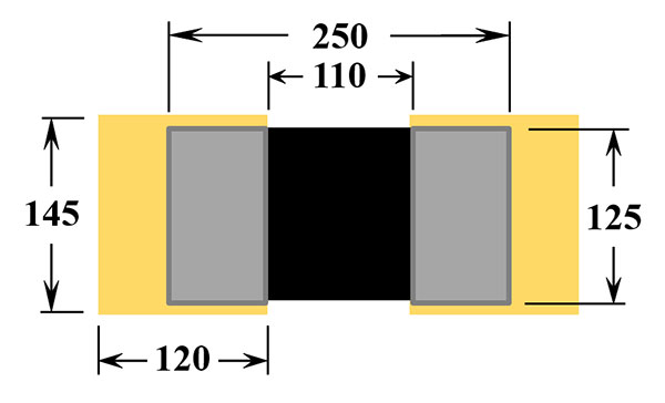
Figure 1. M0201 pad design (dimensions in microns).
Groups of pad sets are ganged together and located within a larger common solder mask window opening. The pad sets are designed as isolated dummy features with no integrated signal path surface trace or embedded via structures for continuity test. Identical clusters of 30 M0201 components are located at four diagonally opposing quadrants on the test board (FIGURE 2).
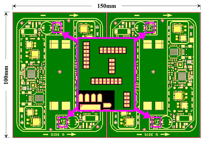
Figure 2. M0201 pad locations on test circuit board.
Our first laser-cut printing stencil was designed at 80µm thickness. This stencil, however, was stepped down to 50µm thickness for the two left-positioned clusters of M0201 components. All M0201 pads were designed with 120 x 140µm size rectangular stencil apertures, which measures nearly the same size as the pad. A Type 5 no-clean SAC 305 solder paste was printed at a speed of 50mm/sec. using 170mm size ultrasonically powered 60° squeegees operated at a pressure setting of 4.6kg. The intentional use of such squeegee technology was motivated by its unique ability to improve paste transfer efficiency for small aperture sizes previously demonstrated down to 0.4 area ratio.2
Key learning outcomes from this printing-focused test included observing excessive print deposit volume occurring through the apertures located in the stepped locations on the stencil, which we attributed to improper squeegee contact to the foil inside the step regions. The stepped locations were determined to be too small to permit the squeegee to effectively wipe the stencil surface clean. The size and volume of the solder deposits printed through M0201 apertures using the full thickness portion of foil were expected to print more poorly in comparison due to an unfavorably low area ratio of 0.4. The results, however, were in fact dimensionally quite similar to the prints originating from the stepped apertures (FIGURE 3). We believe the position of the aperture gasket has much to account for this larger-than-expected print volume outcome. As referenced in FIGURE 4, the solder mask influence on the contact position of the aperture gasket can impact the quantity of solder particles printed. We expect the M0201 aperture will not be in direct contact with the pad, which leads to printing a solder surplus volume.
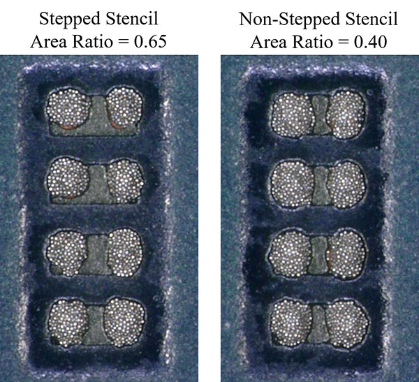
Figure 3. M0201 print deposits from the first assembly test comparing stepped and non-stepped stencil results.
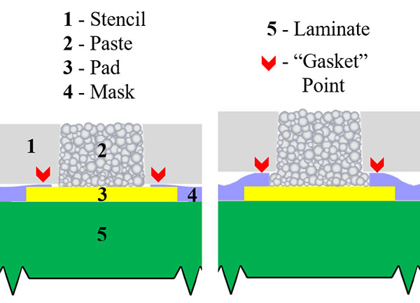
Figure 4. More print volume results when the stencil gasket point is further away from the pad.
Previous accounts of the stencil print focused investigation have been documented.3 Given that the printed volume of solder paste appeared sufficient, perhaps even excessive, a follow-up study added M0201 component placement and reflow using the same printer setup inclusive of solder paste and stencils. Our expectation to witness faults and failures was surprisingly hushed, as the eight assembled boards containing 960 M0201 components exhibited zero reflow defects. However, upon reviewing the reference images of placed components in freshly printed solder paste, the clear majority of them had displaced the solder deposits toward each other along the underside of the components. At a minimum, the paste spread to alarmingly close inter-spacing, and at most severe, bridged conditions were seen (FIGURE 5). Still, all the reflowed results were remarkably defect-free. Further details of this work can be found in Whitmore and Schake.4
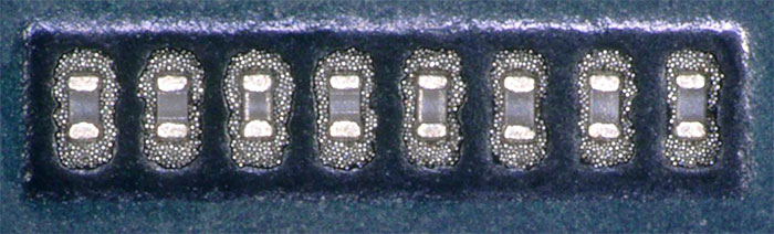
Figure 5. M0201 components placed in wet paste from first assembly test.
While on one hand the reflowed results indicate success, we are nonetheless uncomfortable to endorse a printing process that produces prevalent wet paste bridging upon placement of components. The reflowed solder joints in principle appear acceptable per IPC-A-610E, but their form is considerably bloated.5 Our judgment is the fillets are too large (FIGURE 6). Printing a considerably reduced solder paste volume became the objective of our ensuing work.
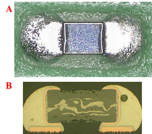
Figure 6. Swollen solder fillets on assembled M0201 component; top view A and cross section perspective B.
Low Area-Ratio Printing
Our motivation to print less paste volume is to discourage wet solder bridging across the pads under placed M0201s and to encourage formation of concave solder joint fillets on component terminations instead of convex. On the surface, this objective seems feasible, but upon imposing a stencil design boundary condition to fix the stencil thickness at 80µm, this task seems impractical. The reasons to fix the stencil thickness at 80µm include:
- We consider this to be the thinnest foil that can still accommodate printing enough solder paste to support common legacy components included on modern high-density mobile product assemblies.
- A thicker stencil will make it more difficult to print M0201s, causing radically low area-ratio aperture designs.
- A stepped-stencil design was found incompatible for our board design (due to layout and density), as we could not successfully print the step isolated M0201 components.
From our previous M0201 assembly experience, 120 x 140µm size stencil apertures produced prints containing too much solder paste volume.4 From this experience it is logical to consider reducing the aperture size to shrink the print deposit volume. This approach, however, leads to stencil aperture area ratios located even further to the left of 0.4, heading the wrong direction on that scale with respect to published industry standard stencil design guidelines.6 FIGURE 7 clarifies the relationship between area ratio vs. mean solder paste transfer efficiency. The printer setup can impact capability, leading to better or worse results.
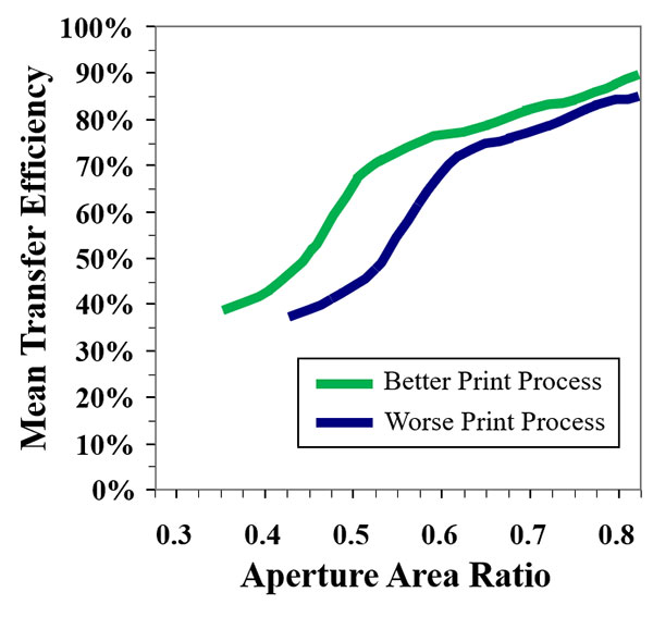
Figure 7. Solder paste print transfer efficiency response to aperture area ratio.
It became clearer our objective here would be to consider printing miniscule aperture sizes we ordinarily would dismiss due to extreme violation of area ratio guidelines. We explored the literature for evidence of printing such low area ratios and identified two references that offered us encouragement to pursue this direction further. In FIGURE 8 the box plot data from Rösch et al for print transfer efficiency occurring below 0.4 area ratio is noted at quite predictably low values, but the print distributions indicated are also quite well controlled.7 In FIGURE 9, histogram print transfer efficiency data from Whitmore et al shows the smallest aperture size at 0.4 area ratio produced a more uniform print volume distribution compared to the adjacent slightly larger aperture size at 0.45 area ratio.8
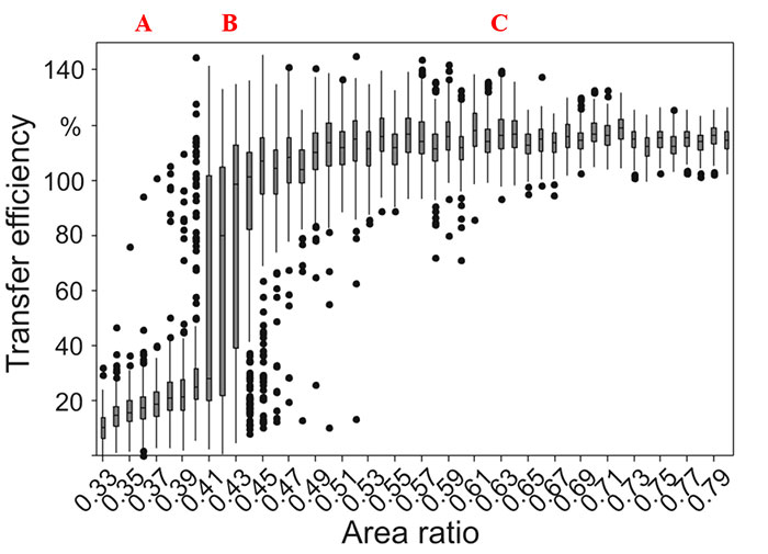
Figure 8. Solder paste print transfer efficiency scatter response to aperture area ratio per Rösch et al.[7]
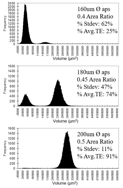
Figure 9. Solder paste print volume histograms per Whitmore et al.[8]
These trends don’t necessarily deviate from expected solder paste printing behavior, but until now we’ve not attempted to critically rationalize printing results at such low area ratios. A closer view confirms some consistency between the two graphs (Figure 8 vs. 9) in achieving quite stable print transfer efficiency (although low) at the smallest area ratios, while the data appear chaotic for the intermediate level area ratios on the scales shown (typically in the area ratio range of 0.4 to 0.45). Based on this analysis a simplified form of the Rösch plot from Figure 8 is drawn in FIGURE 10, where we claim relatively uniform low-volume printing results can be achieved at preposterously small area ratio aperture dimensions.
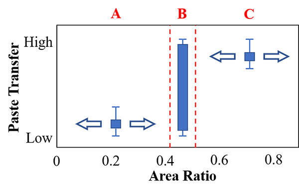
Figure 10. Solder paste print transfer scatter trends, simplified model.
Dissecting the Transfer Efficiency Curve
The classic area ratio vs. transfer efficiency curve has existed for decades and is routinely cited in published stencil printing research. One of the earliest references to this comes from Markstein.9 Per closer view of Figures 8 and 10, the solder paste transfer efficiency behavior can be divided into three distinctive regions: repeatably high paste transfer for high area ratios (sector C), repeatably low paste transfer for low area ratios (sector A), and high scatter paste transfer for in-between area ratios (sector B). The capability to print and successfully transfer any solder material from very tiny aperture holes is largely credited to cohesive paste detachment occurring as the board separates from the stencil after the squeegee completes a printing stroke. This is considered the overwhelmingly dominant print response occurring for very small area ratio apertures. Discovery of archived research supports this model per FIGURE 11, where scaled up experiments characterizing solder paste release from manually filled large tubes provided clear visualization of this behavior.10
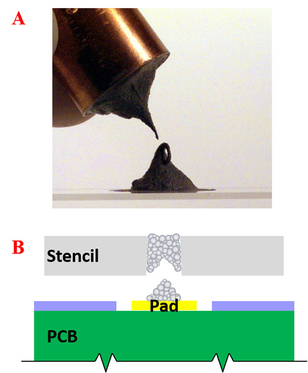
Figure 11. Paste release from clogged aperture; scaled up experiment A [10] and theoretical representation B.
Printing Evaluation
Given adequate evidence in the literature that printing non-sensibly sized stencil apertures offered a realistic possibility to print a controlled low-volume level of solder particles, we decided to press ahead with print trials incorporating several novel stencil aperture designs. One of our guiding principles was to expand on the aperture “disruptor” strategy originally proposed by Ashmore11 and consider several alternative exotic aperture geometries to coax more repeatable print deposit formation. TABLE 1 lists examples of some of these aperture designs.
Table 1. Selected Aperture Designs for Print Testing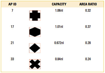
The initial print trials on Cu blank panels attempted to use solder paste inspection (SPI) equipment to quantify results. Due to the diminutive size of print deposits occurring, the SPI threshold level was reduced to the lowest level that still produced acceptable gage data (@15µm for our system). However, even at this setting the tool still falsely reported numerous completely missing deposits when in fact solder particles were visibly printed. Lacking full confidence in SPI capability, we were compelled to evaluate results more strictly against qualitative inspection criteria.
Our first impression concerning print quality from these low area-ratio aperture designs was the prints, albeit low paste transfer, were visually quite repeatable. When comparing ultrasonically powered squeegee results against standard squeegee results, we observed ultrasonic squeegees produced slightly fuller average size deposits, fewer completely missing deposits, and showed better control of print volume distribution among groups of deposits (FIGURE 12).
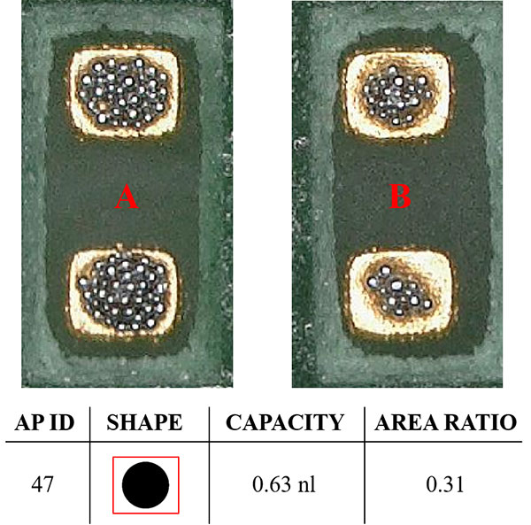
Figure 12. Typical print deposit profiles using ultrasonically powered squeegees (A) and standard squeegees (B) from Aperture ID 47.
Several iterations of stencil design were evaluated for printing performance, which included 47 unique aperture designs. We determined from qualitative comparisons of print results that our exotic aperture designs did not print significantly better than more commonly designed shapes. Our cut to the final four aperture designs included those identified in TABLE 2, which were then implemented on the proper assembly stencil pattern that included apertures to print all the components on our main logic mobile phone product assembly test circuit board. The materials and machine setup used for both stencil print characterization and subsequent M0201 assembly validation testing are identified in TABLE 3.
Table 2. Aperture Designs Selected for Assembly Test 2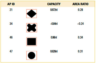
Table 3. Stencil Printer Setup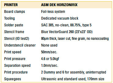
Assembly Trial Results
The materials, equipment and procedure for assembly testing were exactly the same as used from our previous trial reported in Whitmore and Schake,4 with two exceptions. First, the circuit board used in this follow-up test was manufactured by a different vendor under a few amended construction details we felt were important to improve overall quality. The main differences specifically influencing M0201 pads here include tighter tolerance specification to designed pad dimensions, laser-direct imaged (LDI) solder mask openings (designed slightly larger and requested slightly thinner) instead of liquid photoimageable (LPI), and ENIG pad finish instead of Cu OSP (FIGURE 13). The second exception to spotlight concerns the fundamental subject of this research: using different M0201 component stencil apertures designed with “impractically” small area ratios to print very low paste volume (Table 2). This stencil was laser-cut on 80µm-thick stainless steel fine-grain type foil material, contained no step areas, and did not have any flux-repelling coating chemistry applied. A simple assembly validation test comprised eight reflowed boards, each populated with M0201, M03015, 01005, 0.8mm pitch BGA, and 0.5mm pitch QFN components. Build conditions for the eight assembled boards are explained in TABLE 4.
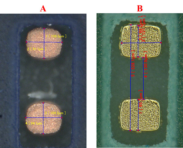
Figure 13. M0201 pads. A - original board, Cu/OSP pads. B - new board, ENIG pads.
Table 4. Assembly Validation Test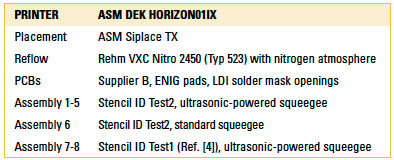
As the facility hosting our assembly test functions to provide demonstration, training, and assembly process development services, all equipment used was state-of-the-art and optimally maintained while in operation under highly skilled supervision.12 While this setup itself did not guarantee a successful outcome, it did ensure a well-controlled assembly process, offering the best opportunity to achieve a successful outcome in our limited scale build. The printing results were found to mimic numerous rehearsals, and placement largely adhered to expectations. There were no observations of missing solder paste on any M0201 pad, despite the low area-ratio aperture designs used. Also, there were no occurrences of print bridging defects on any board. Note during this small-scale trial that the understencil wiping function on the printer was disabled, as the visually repeatable print quality achieved did not warrant using it. The placement machine was programmed to mount M0201s on the board using a default placement force recipe, whereby the components are pushed into the solder paste to firmly contact the pads. As predicted, solder paste bridging was observed to occur for M0201 components placed onto pads containing a high level of printed solder paste volume. This was the only visible placement concern noted, as all components were positioned correctly in wet paste. Upon our examination of all the reflowed boards, to our surprise there were no M0201 components exhibiting solder short defects, despite many of them containing large, bulging solder fillets. In fact, all assembled M0201 components reflowed properly, with no discernable open circuits (e.g., tombstone, drawbridge) or extraneous solder ball occurrences.
The M0201 component locations on all eight assembled boards were photographed following stencil printing, component mounting and reflow. Several mounted M0201 components representing a range of solder print volumes were ultimately cross-sectioned to investigate and compare solder fillet formations. Selected examples of these are offered in FIGURE 14, representing solder joint volume classifications of excessive, ideal, fair and poor.
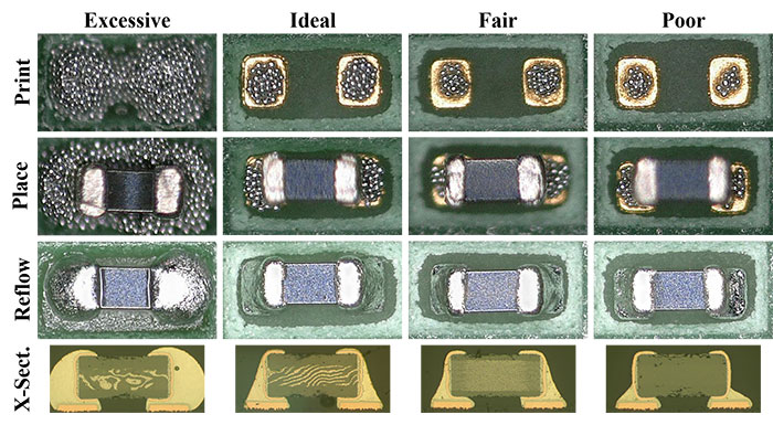
Figure 14. Example outcomes from M0201 assembly test.
Conclusions
We have identified a specific challenging mobile product-like application containing M0201 component pads and imposed the restriction to use a minimum 80µm thickness non-stepped stencil foil to satisfy heterogeneous assembly. Upon exhausting more rational process options, the direction of this research took a surprising path to pursue investigation of stencil printing tiny stencil aperture dimensions largely considered impossible to print. This work featured using stencil apertures designed below an area ratio value of 0.4 that were demonstrated to provide appropriate solder volume accommodating successful assembly of M0201 capacitor components in a highly controlled limited batch assembly process. While this success is groundbreaking insofar as implementing critically low area-ratio apertures, the practical use of such stencil designs in formal manufacturing processes is still highly discouraged. Further assembly investigation using critically low-aperture area ratios should include more rigorous validation testing with scope to capture process boundary conditions.
Interest in pushing the limits of stencil printing is expected to grow as miniaturization continues to evolve and expand. As we’ve learned from this work, such demands oblige exploration of all (even counterintuitive) options, including reconsideration of best working practice guidelines (i.e., stencil aperture design) leading to either reinforce recognized rules or realize new process capability potential.
References
1. Murata Manufacturing Co., “GRM01121C1E100JE01 (008004, CH, 10pF, DC25V),” Reference Sheet, p.25.
2. M. Whitmore and C. Ashmore, “New Developments in Broadband Printing Techniques,” Proceedings of SMTA International, October 2010.
3. J. Schake and M. Whitmore, “Stencil Printing Sustainability for M0201,” Proceedings of the International Conference on Soldering and Reliability (ICSR), May 2016.
4. M. Whitmore and J. Schake, “Stencil Printing Techniques for Challenging Heterogeneous Assembly Applications: Parts 1 & 2,” Proceedings of SMTA International, September 2017.
5. IPC-A-610E, Acceptability of Electronic Assemblies, April 2010.
6. IPC-7525B, Stencil Design Guidelines, October 2011.
7. M. Rösch, J. Franke, Ph.D., C. Läntzsch and G. Kleemann, “Characteristics and Potentials of Nano-Coated Stencils for Stencil Printing Optimization,” Proceedings of SMTA International, October 2010.
8. M. Whitmore and C. Ashmore, “Developments in Stencil Printing Technology for 0.3mm Pitch CSP Assembly,” Proceedings from IMAPS 44th International Symposium on Microelectronics, October 2011.
9. H.W. Markstein, “Controlling the Variables in Stencil Printing,” Electronic Packaging & Production, February 1997.
10. J. Schake, “Solder Paste Release from Real and Scaled-Up Stencil Apertures,” CSP/DCA Consortium, Universal Instruments Corp., June 1998.
11. C. Ashmore, “Unlocking the Mystery of Aperture Architecture for Fine Line Printing,” Proceedings of IPC Apex Expo, February 2017.
12. asm-amt.com/en/center-of-competence
Ed.: This article was first published in the SMTA International 2018 Proceedings and is used here with the authors’ permission.
is senior engineer and is senior manager, Advanced Print Technologies, at ASM Assembly Systems; jeff.schake@asmpt.com.


