As-Shipped vs. Mounted Height for BGA and LGA Packages
A methodology to calculate solder joint height is used to conduct a tolerance analysis on BGAs.
Laminate-based RF modules for wireless applications typically have relatively small body size (<8mm) and LGA-style package terminals. In some applications, BGA-style packages are utilized as a way of populating both sides of the module substrate.
For any given application, the end-product manufacturer will specify a maximum as-shipped component size. The x- and y-dimensions determine the areal packing density on the product motherboard. The z-dimension determines the thickness of the end-product. Components often need to fit under an electromagnetic interference (EMI) shield or other mechanical obstruction.
The component supplier specifies a package outline drawing. When the component is surface-mounted to the end-product motherboard, the x- and y- dimensions do not change. However, the z-dimension (or height) does change. For an LGA component, the height increases due to the printing of solder paste and reflow during the SMT process. For a BGA component, the height decreases due to the collapse of the balls and new shape they attain during the SMT process. This ball collapse occurs despite the printing of solder paste during SMT.
The present study compares the as-shipped vs. mounted height of BGA and LGA packages for a typical RF module design rule set. It is shown that a BGA package should be specified with a 60µm greater as-shipped thickness to end up with the same mounted height as an LGA package. This increase in as-shipped thickness can enable greater electrical performance and reduce quality risk.
Component Terminal Design
An example of a double-sided BGA package is shown in FIGURE 1. One side of the module substrate is populated with active and passive elements, then encapsulated in mold compound. The opposite side of the module substrate has a single underfilled die and a ball grid array matrix.
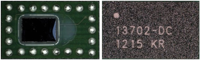
FIGURE 1. Double-sided ball grid array.
An example of an LGA package is shown in FIGURE 2. One side of the module substrate is populated with active and passive elements, then encapsulated in mold compound. The opposite side of the module substrate has an LGA terminal pattern.
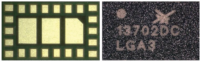
FIGURE 2. Land grid array.
The BGA terminal design used in this study is shown in FIGURE 3. In this application, the raw ball diameter was matched to the solder mask opening. Balls are attached using an automated flux-place-reflow-clean system. The resulting solder height is shown in FIGURE 4.
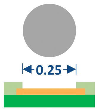
FIGURE 3. BGA terminal design. 0.25mm diameter solder mask-defined pad and 0.25mm raw ball diameter.
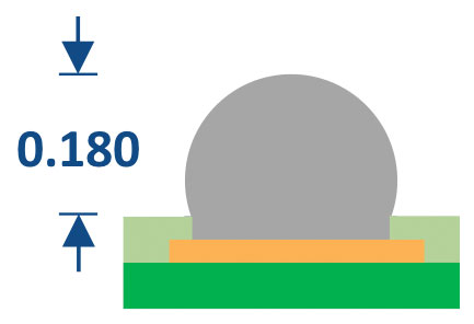
FIGURE 4. 0.180mm solder height after ball attach.
The LGA terminal design shown in FIGURE 5 is typical but can have some variation depending on the function of the terminal (ground vs. signal).
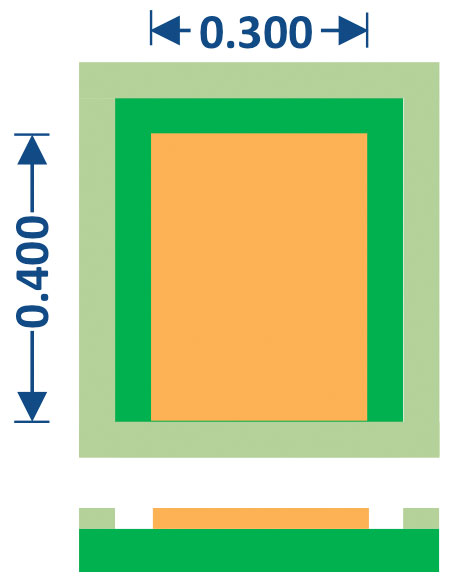
FIGURE 5. LGA terminal design. Metal defined on three sides.
Test Board Terminal Design
The test board terminal design for the BGA case is shown in FIGURE 6. In this application, metal-defined pads were used that matched the diameter of the component terminal solder mask opening.
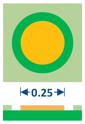
FIGURE 6. BGA motherboard pad design. 0.25mm diameter metal-defined pad.
The test board terminal design for the LGA case is shown in FIGURE 7. In this application, metal-defined pads were used that matched the component terminal size.
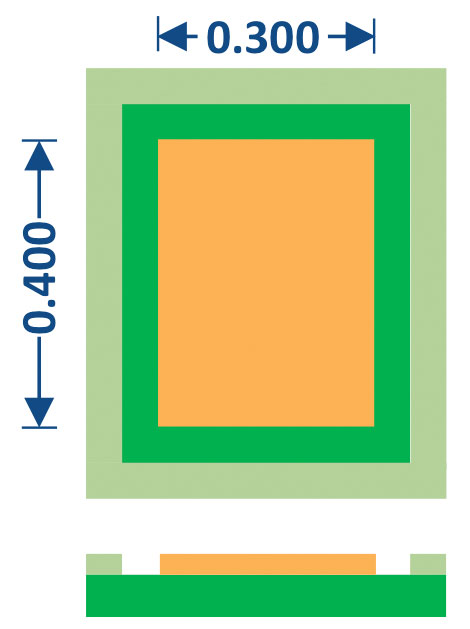
FIGURE 7. LGA motherboard pad design, metal-defined.
SMT Process
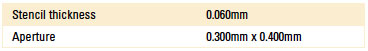
A standard SMT process of print-place-reflow was used to mount components to motherboards. The stencil designs are shown in TABLES 1 and 2.
Table 1. BGA Stencil Design
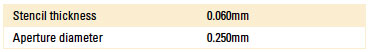
Table 2. LGA Stencil Design
Solder joint height after SMT. The solder joint height (or standoff) was determined in two ways: 1) cross-section, and 2) z-microscope measurement at all four corners and the center of the component. For the BGA case, 50 units from 28 lots of material on 13 different components were characterized. The average solder joint height was 0.145mm (FIGURE 8). For the LGA case, the average solder joint height was 0.025mm (FIGURE 9).
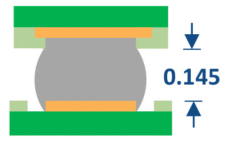
FIGURE 8. 0.145mm BGA mounted height.
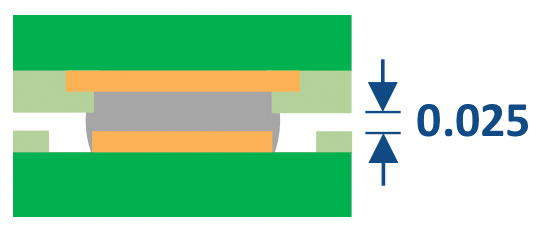
FIGURE 9. 0.025mm LGA mounted height.
As-shipped vs. mounted height. The decrease in BGA height with SMT was 0.035mm (FIGURE 10). The standard deviation on all the measurement data was 0.003mm. The increase in LGA height with SMT was 0.025µm, as shown in FIGURE 11. Based on these results, it is recommended the specified as-shipped BGA thickness should be 0.060mm greater than the specified as-shipped LGA thickness. This increased thickness allowance can be used to improve electrical performance by 1) enabling taller, higher Q inductors, and 2) reducing the coupling between wire bonds and components with the package conformal shield.
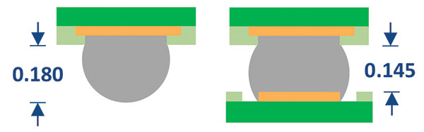
FIGURE 10. 0.035mm BGA decrease in height with SMT.
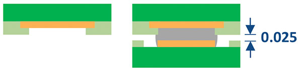
FIGURE 11. 0.025mm LGA increase in height with SMT.
Calculation of Solder Joint Height
Solder ball and solder joint height can be estimated with fair accuracy using basic geometric equations. In most cases, the weight of the component is negligible, and the surface tension of the solder is sufficient to force the joint into a truncated spherical shape. Solder mask openings and metal-defined pads can be approximated as cylindrical shapes.
The volume of a cylinder is given in Eq. (1)
Vcyl = hπr2 (1)
Where h is the height, and r is the radius.
The volume of a sphere is given in Eq. (2)
Vsph = (4/3)πr3 (2)
Where r is the radius.
FIGURE 12 shows a cross-sectional view of a truncated sphere. This is the general case where the radius at the top does not necessarily equal the radius at the bottom.
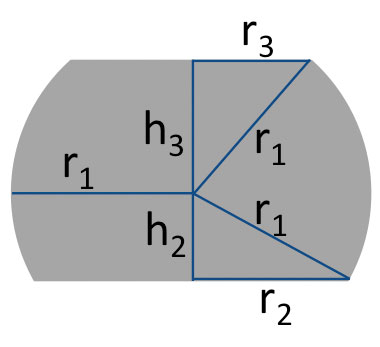
FIGURE 12. Cross-section of a truncated sphere.
The volume of truncated sphere is given in Eq. (3)
Vtru = (h2/6) π(4h22+6r22) + (h3/6)
π(4h32+6r32) (3)
where h2, h3, r2, and r3 are defined in Figure 12.
Depending on the terminal design used on the component and motherboard, one can get a range of possible joint shapes that are a combination of cylinders and truncated spheres (FIGURE 13).
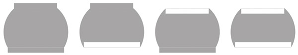
FIGURE 13. Cross-section of various BGA solder joint shapes.
The rule for conservation of volume is given in Eq. 4. The typical assumptions are 1) the solder paste metal volume is 50% of the stencil aperture volume, and 2) there is minimal voiding in the solder joint.
Vraw ball + Vsolder paste metal = Vsolder joint (4)
The left-hand side (LHS) of Eq. 4 represents the solder volume before SMT, and the righthand side (RHS) represents the volume after SMT. To calculate the solder joint height after SMT, substitute Eq. 2 for the raw solder ball volume and Eq. 1 x 50% for the solder paste metal volume. For the RHS of Eq. 4, start with Eq. 3 for the truncated sphere, then add or subtract volume on the top and bottom of the joint using Eq. 1 to account for the terminal design on the component and motherboard.
For example, if we have the second joint shape in Figure 13 (solder-mask-defined package terminal, metal-defined motherboard terminal), the resulting equations to solve are
Vsph(raw ball) + 0.5Vcyl(stencil ap) = Vtru + Vcyl(pkg) – Vcyl(mb) (5)
(4/3)π rraw ball3 + 0.5hstencil apπrstencil ap2 = (h2/6)π(4h22+6rmb2) + (h3/6)π(4h32+6rpkg2) + hpkgπrpkg2 – hmbπrmb2 (6)
where rraw ball is the raw ball radius, hstencil ap is the stencil thickness, rstencil ap is the stencil aperture radius, hmb is the motherboard pad thickness, rmb is the motherboard pad radius, hpkg is the package solder mask thickness, and rpkg is the package solder mask opening radius.
All the variables in Eq. 6 are known, except h2 and h3. Since rmb and rpkg are known, we can derive an equation that relates h2 and h3 by using the geometry shown in Figure 12.
rmb2 + h22 = r12 = rpkg2 + h32 (7)
h22 = rpkg2 + h32 - rmb2 (8)
Eq. 8 can be substituted into Eq. 6 to get an equation that has a single unknown, h3.
(4/3)πrraw ball3 + 0.5hstencil apπrstencil ap2 = ((rpkg2 + h32 - rmb2)0.5/6)π(4(rpkg2 + h32 - rmb2) + 6rmb2) + (h3/6)π(4h32+6rpkg2) + hpkgπrpkg2 – hmbπrmb2 (9)
Eq. 9 can be solved in an iterative manner by incrementing the value of h3 until the LHS is equal to the RHS. Once h3 is known, h2 can be determined from Eq. 8, and r1 can be determined from Eq. 7. The solder joint height (or standoff) is equal to h2 + h3.
This methodology has been used by the author since ~1990 to predict the height of flip chip and BGA solder joints ranging from 0.040mm to 1.50mm pitch design rules. It is generally accurate to within 10% or better.
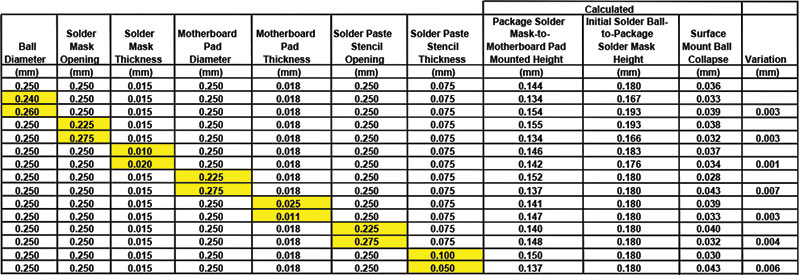
The BGA solder joint height was calculated for the baseline case and several variants (TABLE 3). It is seen that the baseline case is in good agreement with the measured results shown in Figure 10. Each variable in Eq. 9 was adjusted high and low in accordance with typical manufacturing tolerances. The resulting variations in solder joint height and ball collapse were calculated. By adding the variations using root sum squared method, the total variation in ball collapse during SMT is expected to be +/-0.012mm. This is approximately +/-4 standard deviations in the measured ball collapse data.
Table 3. Calculated Solder Height
Conclusions
- The as-shipped vs. mounted height of BGA and LGA packages was compared for a typical RF module design rule set.
- The BGA height decreases by 0.035mm after SMT.
- The LGA height increases by 0.025mm after SMT.
- The specified as-shipped BGA thickness should be 0.060mm greater than the specified as-shipped LGA thickness. This increased thickness allowance can be used to improve electrical performance by 1) enabling taller, higher Q inductors, and 2) reducing the coupling between wire bonds and components with the package conformal shield.
Ed.: This article was first published at SMTA International and is republished here with permission of the authors.
, , and are with Skyworks Solutions
(skyworksinc.com); robert.darveaux@skyworksinc.com.


