I’m a Board Test Engineer and I’m Loving It!

Life on the road can be relentless, but it’s never boring.
I was recently mulling on the pending end to 2014 when a coworker asked what I thought of my life as an engineer. My life as a board test engineer? I’m swamped, but wow, what a swim!
Every day is an adventure and, despite 27 years of work experience, I’m still learning new things, from managing projects and customer requests to implementation of the latest test technologies. Inside the life of a board test engineer is a wide variety of responsibilities and expertise needed to maintain relevance in a very competitive market where technology evolves as fast as the new product shipping out.
The array of products tested in electronics manufacturing is more than enough to keep board test engineers motivated. Just imagine the millions of printed circuit board assemblies (PCBA) for smartphones, tablets, computers, network servers, LED televisions, industrial tools, home appliances, automotive electronics and even medical equipment … the list goes on.
The best thing about my job is that I get to work on amazing leading-edge manufacturing board test solutions, such as the latest in in-circuit test (ICT), boundary scan test and even innovations like Intel Silicon View Technology. Let me briefly describe these technologies.
ICT is essential, used to test electronics components in a PCBA, to detect manufacturing-related defects such as short, open or wrong/defective components. In essence, it’s an electrical process test to ensure all signals go as they should.
Boundary scan or 1149.1 is an IEEE standard that enables testing of a PCBA by utilizing the boundary scan cells that are embedded in a pin of an integrated circuit (FIGURE 1). The boundary scan test solution is not limited to testing opens and shorts between the interconnection of ICs with a boundary scan cell. It can also test interconnections between ICs without boundary scan, and be used to program memories or even execute a built-in self-test.
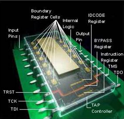
Figure 1. Boundary scan or IEEE 1149.1.
Intel SVT, a proprietary Intel test technology, enables testing of motherboard PCBAs that use Haswell CPUs. In such board architectures, test access is constrained by PCBA real estate or high-speed signal, limiting access needed if ICT were used. With new technologies such as the x1149 boundary scan analyzer, the only test access required is the debug port2, and using Intel DFx* Abstraction Layer (Intel DAL) to securely access the Haswell CPU silicon to verify its function and that of surrounding devices.
My job enables me to travel to places where most people go for their holiday destinations. For me though, sightseeing is done en route to the customer site. Traveling means spending a good part of my time on the customers’ manufacturing floor, debugging a test, testing a new system feature or software release. Most evenings, work continues inside my hotel room doing teleconferences for test developments, reports or simply replying to emails.
Being a self-proclaimed gourmand (yes I love to cook, and am pretty awesome at dishing up gourmet numbers), I consider cross-continental cuisine as a perk as I get to taste food from all over the world. However, most meals are done in a rush. I have also become adept at driving different car models, switching easily between left- and right-hand drive within the span of two airports.
The most exciting part of this job is attending international test conferences to learn what competitors offer and, of course, to socialize with fellow test engineers; it’s back to the fraternity feel on such occasions where we can swap tales and jokes in test lingo without the other party throwing a blank face back at me! With all this flying around, I clock enough mileage to make up for missed family time with free airline tickets for a real holiday once in a while.
Call it mobile computing, or mobile commuting. I can basically work anywhere – from the comfort of my home or out in the park. Modern technologies allow us to physically work anywhere in the world, with my laptop, smartphone and software connecting me with my company servers and global colleagues.
Like most of my colleagues, I like gizmos, and I think the smartphone is probably one of the most productive toys invented in recent times. It enables most people to get connected via various social media. I manage to enjoy my smartphone, using it to update our ICT product page on Facebook, and use WhatsApp and LinkedIn to stay connected with fellow engineers around the world (FIGURE 2).
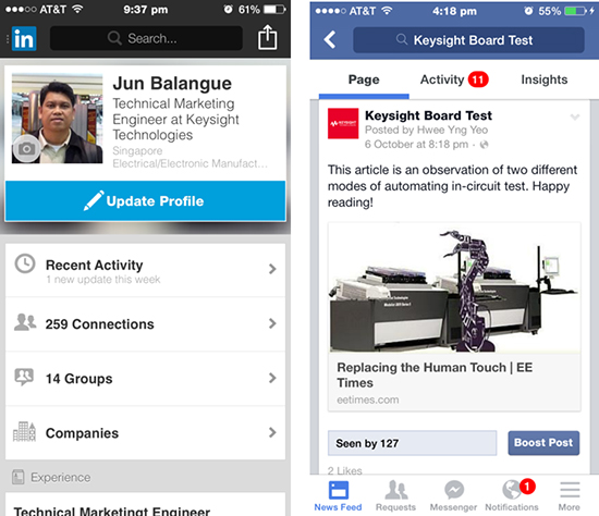
Figure 2. LinkedIn and Facebook are two of the ways I stay connected with colleagues.
Most of the time, I work alone and can be oblivious to my surroundings. But I have many friends whom I can count on when in need of technical help. My smartphone and laptop enable me to call and chat with colleagues and global customers or visit technical forums to search for solutions, literally at my fingertips.
The life of a board test engineer is nothing like what many perceive it to be: a boring deskbound job. It offers both great challenges and opportunities. At the end of the day I find great satisfaction knowing that when I login to another day at work, I have made a contribution to change the world of technology, and my small role in the grander scheme of things has actually made life easier for someone, from fellow manufacturing engineers, right to the end-users, like you and me, connecting via this increasingly seamless world of electronics.
is a technical marketing engineer at Keysight Technologies (keysight.com); jun_balangue@keysight.com. The former Agilent Technologies Electronic Measurement Group is now Keysight.


