The Flash Programming Flow

On-board flash memory device testing and programming.
Memory capacities are one of the important product specifications consumers review before buying a product. An increasing number of memory devices are being packed into electronics products, and a single malfunction could cause gross failure across the devices.
Hence, flash memory testing and programming have become indispensible to the quality check during different product development phases.
This month, we focus on how on-board flash memories are being tested and programmed at different stages of product development and manufacturing. (The term “on-board” refers to flash memory soldered into the PCB.)
Flash memories are programmed across different stages of the product, from engineering verification and production verification to high-volume manufacturing (Figure 1). During the prototype and engineering verification stages, the R&D and NPI test engineer tests and programs the on-board flash memories. The first step performed is structural test, to ensure that the flash memory is correctly soldered in the PCB and that there are no short or open defects on the flash memory pins.
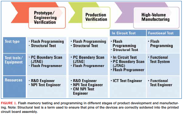
One of the available boundary scan tools that has the capability to simultaneously test and program flash memory is the PC boundary scan device. This has the capability to generate structural test vectors able to verify that the addresses, control lines and data pins of the flash memory are correctly soldered on the PCB. Boundary scan tools make use of the IEEE 1149.1 standard for test access port and boundary scan architecture, commonly known as JTAG.
The PC boundary scan tool offers some advantages worth considering:
- It is easy to implement during prototype by making use of the CPU/ASIC/FPGA boundary scan cell to test and program the flash memory devices connected.
- A bed-of-nails fixture is not needed. Instead, all that is needed are four mandatory pins on the boundary scan device: TDI, TCK, TMS, TDO and the optional TRST.
- New benchtop solutions enable tests or programming vectors developed during prototype and engineering verification to be used during product verification and volume manufacturing.
During product verification, depending on the test strategy used, the PCB with on-board flash memory can be tested and programmed using in-circuit testers or a PC boundary scan tool. The latter can also be integrated directly into the ICT for boundary scan testing and flash memory device programming, and the same test developed for the prototype can be reused during engineering verification.
At the high-volume manufacturing stage, the two important things to look for concerning on-board flash memories are:
- The on-board flash memory is correctly soldered into the PCB.
- The on-board flash memory is programmed with the correct data.
The on-board flash memory is correctly soldered in the PCB. Any open or shorts failure in the flash memory pins might cause a gross failure at the functional test station, such as “no boot” or “hang” symptoms. This will be a failure that is hard to diagnose at the functional test station because other device failures can also exhibit the same symptoms. Besides, if the flash memory is not programmed properly, the PCB might not be able to boot up properly, and the functional test might not be able to proceed, thereby disrupting the rest of the functional test. However, at the ICT stage, the failing devices can easily be diagnosed and repaired, permitting the rest of the functional test to proceed.
The flash test executed at this stage is done using a simple walking one “1” or walking “0” test to toggle the address. The data bus is verified by writing a complementary set of data to ensure all pins are toggles. The control pins such as write enable and output enable of the flash memory are also checked to ensure the pins are correctly soldered on the PCB.
This test can be executed either by using a PC boundary scan tool or an ICT during production testing.
Ensuring on-board flash memory is programmed with the correct data. There are two types of data that can be programmed into the flash memory:
- Static data. The data are fixed and do not change.
- Dynamic data. The data do change and vary from one PCB to another PCB.
It is not advisable to program large amounts of static data in the flash memory using boundary scan silicon nail or via direct programming using the ICT bed-of-nails, as the test time can be very long, and this might affect the production beat rate.
Static data can still be programmed into the flash, however, if they are only a few megabytes, as in those found in firmware needed to enable PCB boot up at the functional test stage, or when dynamic data programming is needed. These examples can be found in the creation of mac addresses, board serial numbers, time stamps, testing history and other variable data.
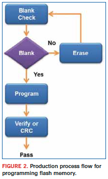
Programming flow for dynamic or static data during production (Figure 2):
- Check the flash memory identification (ID) to ensure the correct device is soldered onto the PCB. This test can also detect address or data failures in the flash device if the read ID does not match the expected value.
- Once the device ID testing is successfully completed, the next step is to check whether the flash memory is blank or if there are no data programmed due to an error.
- A blank test failure is an indication that the flash memory is not blank. An erase step is needed to ensure the flash is ready to be programmed.
- If the device passes the blank test, or if a data erase step has been executed, then the next step is to program the data to the flash memory.
- After programming the data to the flash memory, a Cyclic Redundancy Check (CRC) or verify test is needed to ensure the data have been correctly programmed.
It is good to keep this flash programming flow in mind. Flash memory testing and programming are very important steps of the product development and manufacturing stages. By preselecting the right tools, the entire manufacturing process, from R&D and NPI to that of production verification, will benefit.
Jun Balangue is a technical marketing engineer at Agilent Technologies (agilent.com); jun_balangue@agilent.com.