How Stencil Design and Reflow Profiles Affect Variation in QFN Voiding Data: A Case Study
Is a new standard test needed?
Foreword. I would like to note as an addition to the original text a few topics from frequently asked questions. Originally I had approached this paper as an investigation into several data sets that showed interesting results. It seems to have evolved into an analysis of how a variety of factors will impact voiding results. I see many of these factors echoed in further industry papers, as QFN packages grow in popularity and more projects are published. The common key to success is considering all the potential contributing factors, then controlling most, and optimizing the ones that are mutable. Often it comes down to solder paste material choice and limited process parameters as the main optimizing factors.
Reflow profiling: Some of the investigated cases include a comparison between typical reflow profiles and longer, hotter profiles. It is important to always consider the full assembly when profiling. The cases here are idealized because a test board with only QFN components was used. In the real world, the process window is limited by several factors: component maximum temperatures, oxidation resistance on large components, avoiding graping on small components, etc. When creating an optimal profile for voiding on a real assembly, profiling to minimize voiding must be tempered with attention for the other challenging parts on the assembly.
Stencil design: The stencil designs presented in this paper were chosen to illustrate whether increasing solder volume will decrease voiding. Sometimes, depending on factors like component size, having one large aperture is not favorable. When solder becomes molten, the surface tension of the solder forms a meniscus.
When the aperture design is not separated, this meniscus may be tall enough to permit the component to tip or float, challenging the integrity of perimeter solder joints. The component used here was relatively small, so this effect was not seen.
Component cleanliness: A possible explanation was proposed for the incidence of intermittent high voiding values: Were the components clean? Through further investigation, there was certainly variation in the surface finish of the components. The data sets in this paper were collected over a considerable period of time, so variations in component cleanliness may have contributed to higher incidence of intermittent high voiding values in some data sets. Nonetheless, the trends seen with reflow profile and stencil design stay true.
Standoff height: For geometric calculations, the minimum recommended standoff height was chosen. This is not the default, however. Ample standoff height will improve the ability of volatiles to escape from the solder paste during preheat. Furthermore, decreased standoff height will degrade solder joint reliability because there will not be enough solder material to bridge the gap when CTE mismatches and stresses occur. It is critical to maintain the minimum standoff recommended by the component manufacturer. This can become more challenging when vias are included in the thermal pad design.
Vias: Vias were not included in this test design. This is a critical difference between these material comparisons and most real-life assemblies. If a design has vias in the thermal pad, this drastically changes the approach to stencil design. In the case of designs with open vias, it is preferred to avoid printing solder paste close enough to permit solder to wick into the vias. Depending on the number and size of vias, when solder wicks down them, it can have a significant impact in the solder volume remaining in the solder joint.1 There are also cases where the solder interaction with the vias can contribute to voiding, or result in the component being skewed or tilted, thus affecting perimeter solder joint integrity as well. The industry has pursued several different approaches to this design challenge2, and this is an interesting area for further study.
Introduction
Void reduction in large, confined solder joints has been a hot topic for more than a decade. The affected component may be evolving, but the same challenge exists. Many papers have reviewed process recommendations to lower voiding,3 looked at material modifications to mitigate the issue, and even suggested material additions such as preforms to increase solder volume without adding volatiles.4 These studies agree on a few things: If there is poor wetting (no matter what the cause), there will be an increase in voiding, and if there is insufficient solder volume, there will be an increase in voiding. The second mechanism contributing to voiding is entrapment of volatiles.
Instead of discussing different ways to mitigate voiding, this article studies several cases in which voiding data were collected using a standardized method. The trends in these data sets led to further test method development.
Cases and Procedures
The new product introduction cycle requires plenty of data collection using standardized test methods. Many experimental formulas and benchmarks are tested.
Over the course of many studies, it was evident there were opportunities to improve the standard test for QFN voiding.
The standard test uses a commercially available test vehicle, with 12 QFN components on the reflow-focused side. These components are Amkor MLF68s, 10mm in size, with 0.5mm pitch, and matte tin finish. The test boards were copper with OSP finish.
The data presented in this paper were compiled from several different studies conducted in Indium’s Advanced Materials and Process Development Lab. These studies were not necessarily focused on QFN voiding, but the resulting voiding data showed interesting patterns that led to further investigation. To make sense of these sets, a brief background of each of the studies is referenced here:
Case 1: Material comparison of SAC 305 materials, processed at two different reflow profiles. This testing was conducted with the original stencil designed for the test board.
Case 2: Screening test for several developmental high-reliability alloys with different fluxes. This testing was conducted with the original stencil designed for the board. Data will be shown with two different profiles.
Case 3: Material comparison with low-Ag alloy fine powder. Several combinations were tested using modified stencil designs.
Case 4: Two standard materials, chosen to represent best- and worst-case, with all three stencil designs.
In all cases, paste was stencil-printed onto the test boards at 100mm/s with minimal pressure. Components were automatically placed using placement equipment. The boards were then reflowed in air in a 10-zone reflow oven. The profile was a standard ramp to peak unless otherwise noted.
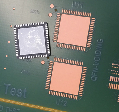
Figure 1. Component and pads on standardized test board.
Stencil Designs
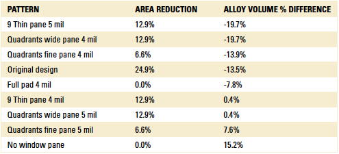
In the component application notes,5 a few stencil designs are suggested, as shown in FIGURE 2, all with varying levels of solder coverage on the thermal pad. The suggested designs break up the solder deposit on the center pad into several deposits. The coverage by area ranges from 37 to 81%.
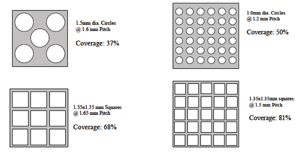
Figure 2. Suggested aperture designs.1
These recommendations take into account considerations for thermal vias in the pad. The test board design has no vias. This removes a large complicating factor from this apples-to-apples comparison test method. For designs using vias, some of this discussion of solder volume will nonetheless apply.
The original stencil design (FIGURE 3) split the thermal pad area into nine square deposits with a wide windowpane pattern. The panes between deposits measured 20 mils thick. Basic area calculations show the coverage by area is 75.1%. This is within the suggested range.
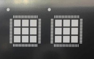
Figure 3. Original stencil design.
When a geometric calculation is made for the 5 mil stencil, assuming solder is approximately 50% solid by volume, the deposit will be 13.5% less than the ideal volume. The ideal volume is based on the pad size and the component application note, which recommends a minimum of 50 microns of standoff for reliability.
A new stencil was designed to increase the coverage of the solder paste and vary the volume of solder to see the impact on voiding results. As shown in FIGURE 4, the four designs chosen were a full pad print, nine windowpanes with finer spacing (10 mils), quadrants with the same finer spacing, and quadrants with 20 mil panes.
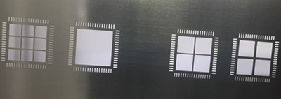
Figure 4. Modified stencil designs.
These designs have a range from 0.0 to 12.9% reduction in solder paste coverage by area. By obtaining both 4 mil- and 5 mil-thick stencils, volumes will range from insufficient to excessive, as tabulated in TABLE 1.
Table 1. Geometric Calculated Values for Coverage by Area and Volume
Results
Case 1 demonstrates a typical data set that was collected using the original 5 mil stencil design. Two profiles were used to demonstrate the low and high side of the reflow profile window.
Figure 3 shows voiding results for four different commercially available solder pastes. Each condition had three associated boards. The voiding results are plotted by component to determine whether any location had an effect on the results. Generally, the higher reflow profile seems to yield lower voiding percentages and lower variation for all four pastes. This result is easily assessed visually; however, it is also clear there seem to be intermittent high voiding results.
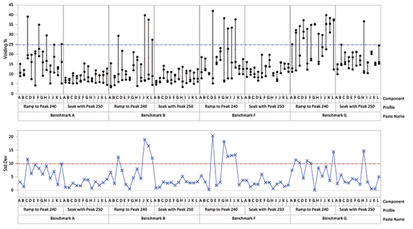
Figure 5. Voiding for Case 1 with the original 5 mil stencil design, showing results at two profiles.
Viewing all the results by profile as distributions (FIGURE 6), there is one group of voiding results that is distinctly higher than the general distribution. Highlighting only benchmark paste A in darker green, the distribution and averages are low, but a couple outliers have voiding >35%. Case 2 is a comparison of several different solder pastes with different flux and alloy combinations. The results in FIGURE 7 are presented by alloy and flux, plotted by component. In this case, two boards were reflowed per paste with a typical ramp to peak profile. Benchmark paste E with alloy 1 shows acceptable results as far as voiding percent, as well as low variation. The experimental formulations do not approach this result. Some pastes show intermittent low voiding components, which led to investigation of the individual x-ray images.
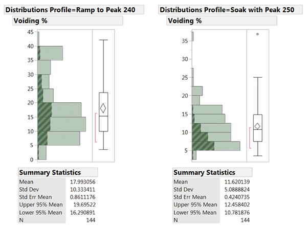
Figure 6. Distributions with Benchmark paste A highlighted.
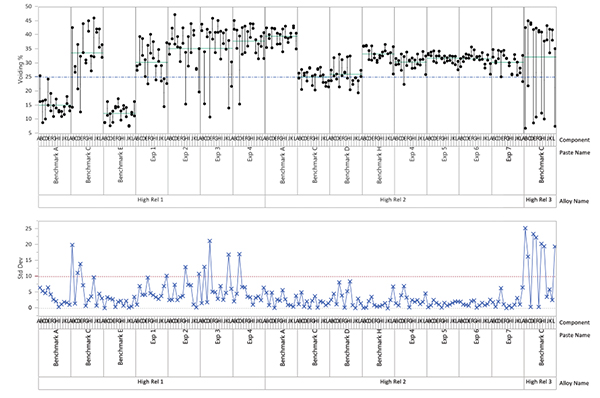
Figure 7. Voiding for case 2 using typical reflow profile and original 5 mil stencil design.
FIGURE 8 shows a selection of component images. The minimum voided component shows different characteristic voiding, depending on the solder paste. The maximum voided component has drastically larger voids. Benchmark paste B’s largest voids do not seem to follow any pattern. Many images of experimental pastes were shown to have a similar “frowny face” pattern. This resembles voids congregating along the pathways created by the nine windowpane pattern.
Benchmark C shows large voids, which almost seem to correspond to the deposits created by the nine windowpane pattern.
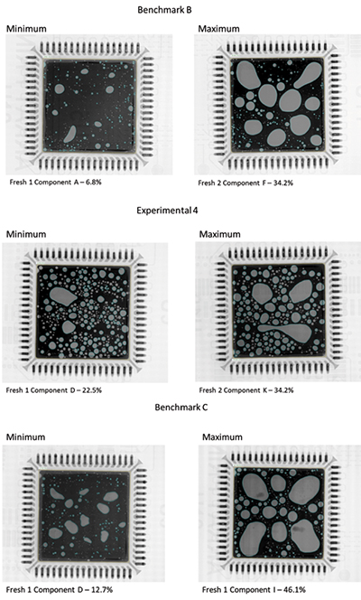
Figure 8. X-ray voiding images from case 2.
Looking back at the maximum voided components in many data sets, the same pattern emerged.
There may be many sources for this variation. Was this trend in the pattern of voiding with this design real? One possible source of this inconsistency was variation in placement height. The placement machine used in this test places components at some height above an ideal zero. Since the board thickness and flatness varies, the amount the component is pressed into the paste could also be a variable. Could the variation be another characteristic of the solder paste formulation? Experimental solder pastes typically showed many small voids and the “frowny face” pattern. These considerations always return to the question of how the solder paste outgassing is affected by the choice of stencil aperture design. This led to development of stencils with new designs, as discussed in the previous section.
With an increase in the solder volume, could these intermittent high voiding levels be mitigated? Would a different pattern with the same amount of coverage yield different results? Overall, the goal was to reduce voiding percentages, mitigate largest voids, and reduce variation in the voiding test results.
Case 3 was conducted on several different fluxes tested with a low-silver alloy. All boards were reflowed using the standard ramp to peak profile. FIGURE 9 shows the variability of the voiding results with the new stencil designs at both thicknesses. Overall, the standard deviation has fallen below 10% for all of the results. There are still a few intermittent high voiding results. When the data are plotted, separating the results by design (FIGURE 10), the intermittent high voiding results do not correlate with a particular stencil or design. The associated x-ray images (FIGURE 11) do not seem to have a common pattern.
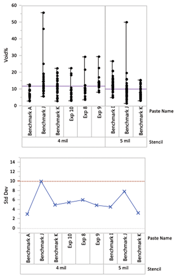
Figure 9. Case 3 summarized voiding results by stencil only.
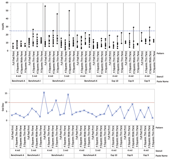
Figure 10. Case 3 voiding results plotted by aperture design.
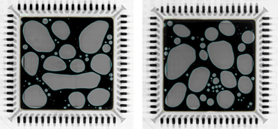
Figure 11. X-ray images of maximum voided components in case 3.
Case 4 simply compares the stencil designs, all other factors being equal. This trial was carried out with two SAC 305 commercially available pastes: one with typically low voiding and low variation, and one with typically higher voiding. The results that were plotted based on stencil and aperture design (FIGURE 12) show relatively consistent results for benchmark paste A. For the other paste, the new 5 mil stencil showed higher variation than either the original stencil or the new 4 mil stencil. The average voiding with new stencil designs was marginally lower. The comparison of variation is slightly skewed because there are more components with the same pattern for the original stencil because the same number of boards was analyzed, but the number of components was not normalized. It may be possible to yield more definitive results with more replicates.
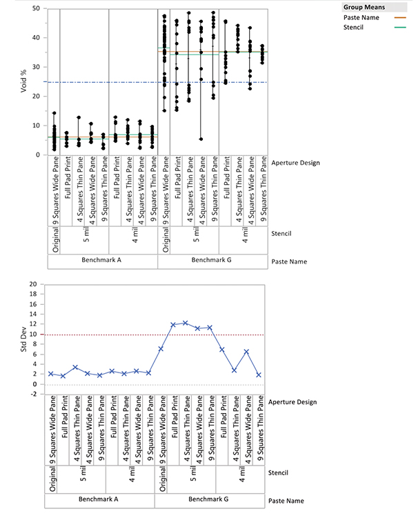
Figure 12. Results from case 4, comparing stencils and aperture designs.
Conclusion
The first case studied was one directed to show the impact of reflow profiling on voiding results. The data presented strongly support lower voiding with a longer, hotter profile. One additional set of results from Case 2, found in FIGURE 13, shows where the profile is varied, but there is little correlation between profile and voiding results. The main difference is Case 2 shows pastes with different alloys, as well as different profiles. Each paste combination may have a different trend.
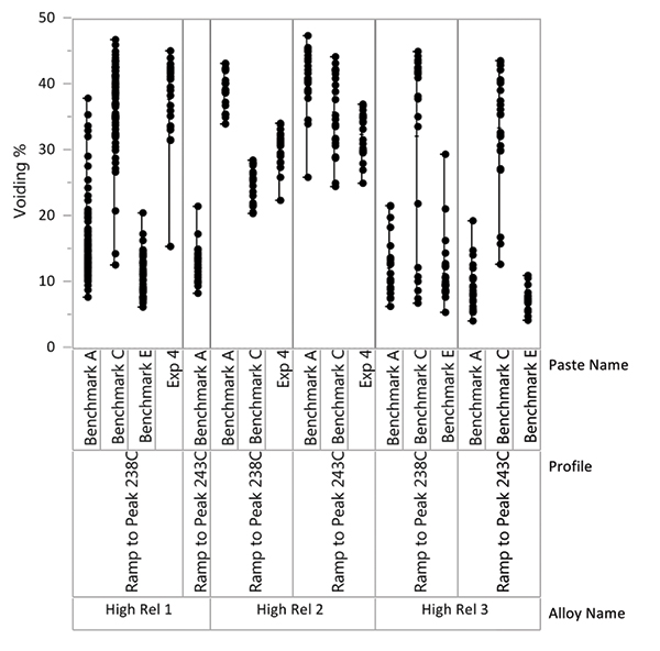
Figure 13. Results from case 2, comparing different profiles.
Generally, the profile influence will have a few general trends resulting in higher voiding:
- If the preheat is too quick, there is not enough time for volatiles to evolve and escape before the solder is molten.
- If the preheat is too quick, the paste can slump, reducing the standoff and preventing the escape of volatiles.
- If the profile is generally too short, volatiles will be more easily entrapped.
- Low peak temperature tends to require more time for complete solder wetting.
- Excessive peak temperature or profile length results in oxidation on surfaces, increasing the potential for voiding.
To reduce the sources of variation in voiding comparison data, two new stencils with four different aperture designs were tested. Generally, these stencils yielded results with less variation than was experienced with the original stencil. The intermittent high voiding results were also less frequent with the new designs; however, some pastes still showed more variation than others.
Designs with higher volumes did not show signs of defects from the excess. (Solder balling or poor fillet formation were the downsides stated in the component application note.5) Designs with less volume (4 mil stencil) did not intrinsically show more voiding or variation. This implies there is not a direct correlation to voiding percent and solder volume. This is especially evident looking at the results for Benchmark paste A in Figure 10, where all stencils and designs show very similar results. This seems to indicate that for some pastes that have a chemistry designed to reduce QFN voiding, the results will also be good for a wide range of designs and conditions.
Acknowledgments
Thanks to Mark Reece and Sarah Bjornland for their assistance collecting much of these data. Thanks to Dr. Arnab Dasgupta for providing many of the experimental formulas.
Ed.: This article was first published at the SMTA International Conference on Soldering and Reliability in June 2016, and is republished with permission of the author.
References
1. Brook Sandy-Smith, “Reliability Challenges for Bottom Termination Components,” SMTA International Conference on Soldering and Reliability, May 2013.
2. Matthew Kelly, et al, “Via-in-pad Plated Over (VIPPO) Design Considerations for Enterprise Server and Storage Hardware,” SMTAI Proceedings, October 2015.
3. Brook Sandy-Smith and Seth Homer, “Optimizing Assembly of QFNs,” SMTAI Proceedings, October 2013.
4. Brandon Judd and Maria Durham, “The Benefits of Flux-Coated Solder Preforms in a QFN Assembly Process,” IMAPS, October 2015.
5. Application Notes for Surface Mount Assembly of Amkor’s MicroLeadFrame Packages, Rev G, September 2008.
is PCB assembly materials specialist at Indium (indium.com); bsandy@indium.com.


