Study of Various PCBA Surface Finishes
A total of nine groups of PCB surface finish were evaluated for solder spread and voiding performance with assembled BGAs and QFNs.
Each of the various printed circuit board surface finishes in use today for lead-free process has its advantages and disadvantages. These surface finishes include lead-free hot air solder leveling (HASL), organic solderability preservative (OSP), electroless nickel / immersion gold (ENIG), electrolytic Ni/Au, immersion silver (IAg), and immersion tin (ISn). Within these surface finishes, OSP, ENIG and IAg are more popular.
Lead-free HASL is not readily available and consistent flatness is difficult. Electrolytic Ni/Au is expensive and, if too much gold is deposited on the pad, can lead to brittle solder joints. Immersion tin shows solderability degradation after exposure to multiple heat cycles, as in a top- and bottom-side PCBA reflow process.
This study evaluated some additional available surface finishes. Electroless nickel/immersion silver (ENIS) intends to replace the gold in ENIG with silver to lower the cost. Electroless nickel/immersion gold with high phosphorus (Hi-P ENIG) intends to provide the highest resistance against corrosive environment.1 Electroless nickel/electroless palladium/immersion gold (ENEPIG) provides excellent solderability for tin-copper-silver based solder alloy.2 A polymer-based coating (PF) that uses the plasma process to deposit was also evaluated.
In addition to ENIS, ENIG Hi-P, ENEPIG, and PF surface finish, OSP and IAg were also evaluated. A total of nine groups of surface finish were evaluated.
Preconditioning on PCB. The PCB with various surface finishes were subject to various preconditioning, to study the effect of each preconditioning in regards to solder spread and voiding performance on BGA and QFN devices.
Preconditioning #1: No preconditioning, assembly is reflowed in air. This is used as baseline.
Preconditioning #2: PCB pre-baked in an oven with temperature of 105oC for eight hours.
Preconditioning #3: PCB pre-baked in an oven with temperature of 155oC for six hours. This is to simulate 1.5 yr. of shelf life.
Preconditioning #4: PCB pre-baked in an oven with temperature of 72oC and 85% RH for eight hours, followed with a bake at 105oC for one hour. This is to simulate more than six months’ shelf life.
Preconditioning #5: PCB goes through reflow oven one time, then assembled.
Preconditioning #6: PCB goes through reflow oven two times, then assembled.
Preconditioning #7: PCB goes through reflow oven three times, then assembled.
Preconditioning #8: Solder paste printed onto PCB, then the solder paste is cleaned off the PCB. This preconditioning holds the PCB for 24 hr. before being assembled.
Preconditioning #9: Same as #8, except the PCB is hold for 48 hr. before being assembled.
Preconditioning #10: Same as #8, except the PCB is hold for 72 hr. before being assembled.
A total of nine different surface finishes were used. The first six consists of OSP, PF, ENIS, IAg, ENEPIG and Hi-P ENIG. Each surface finish has three samples per preconditioning, except ENIS, where only one sample was available for preconditioning #1 to #8. In addition to the first six, PF was added as a topcoat to IAg, ENEPIG and Hi-P ENIG to observe any difference in performance.
Test Vehicle and Assembly Process
The test vehicle in use was the company Multifunction Test Vehicle (MFTV) (FIGURE 1). The solder paste used was no-clean lead-free Sn3Ag0.5Cu (SAC 305) and the board was reflowed in convection oven with air atmosphere using a typical lead-free reflow profile.
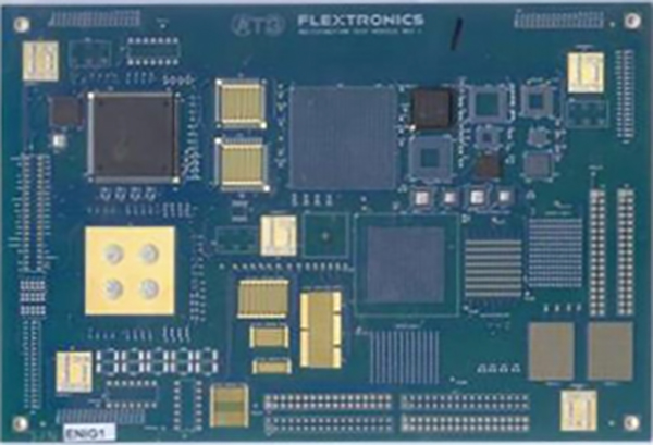
Figure 1. Multifunction test vehicle.
Solder spread test. The solder paste stencil opening was 1:1 to the board pad, except for the area where the solder spread test was used. For the solder spread test, the stencil opening was incremented from 40% to 120% of pad in 5% increments (FIGURE 2). This is on an 80 by 20 mils non-solder mask defined pad.
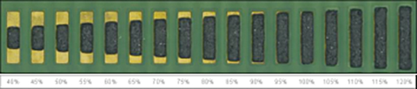
Figure 2. Solder spread test coupon before reflow.
After reflow, each board was visually inspected to identify which pad had the least amount of solder paste coverage that achieved complete wetting. A sample is shown in FIGURE 3, where 55% solder paste coverage had complete wetting.
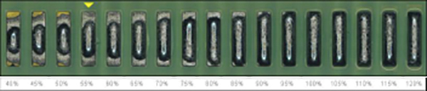
Figure 3. Solder spread test coupon after reflow.
Each test vehicle provides five locations for solder spread test (FIGURE 4). As three samples (except ENIS, only one sample available per preconditioning) were used in each preconditioning scenario, a total of 15 coupons were available for inspection from each surface finish. The results from each coupon were tabulated using statistical software, and a box plot graph generated for each preconditioning scenario. A sample box plot of preconditioning #1 (reflow in air) is shown in FIGURE 5.
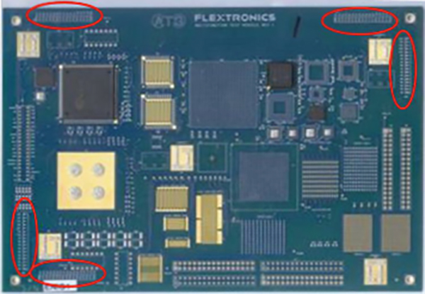
Figure 4. Locations of solder spread test.
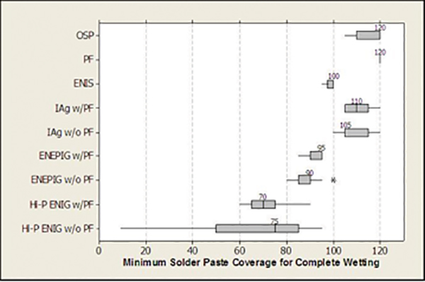
Figure 5. Box plot of solder spread test result from reflow in air.
Based on the data, for reflow in air Hi-P ENIG has the best spread with 70 to 75% solder paste coverage providing 100% wetting. A summary of solder spread results is provided in TABLE 1.
Table 1. Solder Spread Test Results Summary
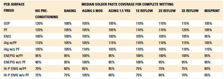
The smaller the solder paste coverage required means better wetting performance. In general, Hi-P ENIG has the best wetting performance across all preconditioning scenarios. No significant difference was found between IAg, ENEPIG and Hi-P ENIG surface finish alone and treated with PF. Both OSP and PF surface finishes required over-print of solder paste to achieve 100% wetting on pad.
Voiding performance of BGA and QFN. The voiding percentage on BGA balls of a 196-pin I/O BGA (U1) and a 64 pins I/O BGA (U300) were measured using a laminography x-ray system. The locations of U1 and U300 are shown in FIGURE 6.
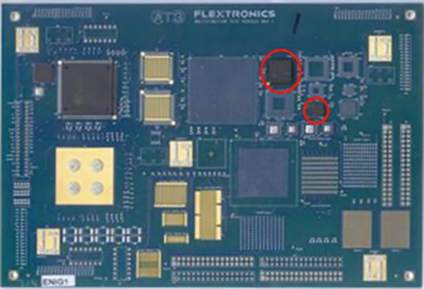
Figure 6. Location of BGAs measured for voiding.
All voiding percentages were below the 25% allowable per IPC-A-610. Both ENEPIG and Hi-P ENIG had the least voiding, at below 4%. All other surface finishes had voiding less than 6%. A box plot of the voiding percentage is shown in FIGURE 7.
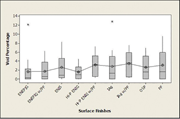
Figure 7. Box plot of BGA pads voiding percentage.
The voiding percentage on the ground pad of QFN/BTC component at U314 was measured using the laminography x-ray system, and the results shown as box plots in FIGURE 8. The QFN ground pad voiding percentage various from 35% to 50%. There was no particular surface finish with significantly less voiding.
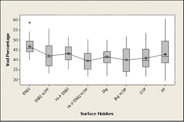
Figure 8. Box plot of QFN ground pad void.
Cross-sectioning. One board from preconditioning #1, #4, and #7 from each surface finish had cross-sectioning performed on QFN/BTC at U314 and BGA at U1. This was to inspect for any abnormal behavior at the interface between component pad to ball, and ball to PCB pad. FIGURE 9 shows the location of QFN/BTC and BGA being cross-sectioned, and where the cut on the component was made. There was no significant difference noticed in the cross-section results between IAg, Hi-P ENIG and ENEPIG surface finish with or without PF. Micro-voiding was noticed on the ball to pad interface for BGA on PF surface finish. This micro-voiding was not found on OSP or other surface finishes (FIGURE 10).
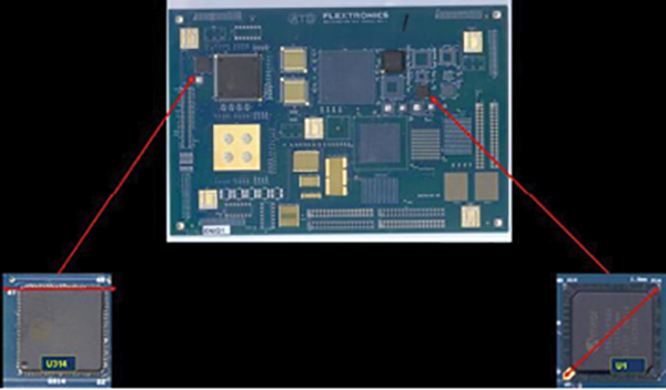
Figure 9. Location of QFN/BTC and BGA cross-sectioned.
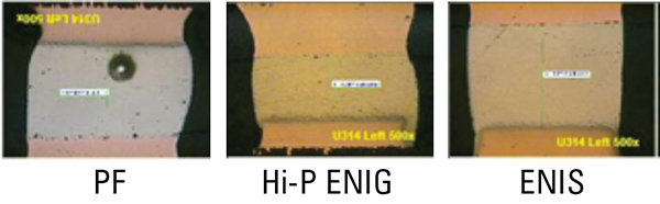
Figure 10. Picture of micro-voiding on PF vs. Hi-P ENIG and ENIS.
During cross-sectioning, the standoff height of BGA at U1 and QFN/BTC at U314 were measured. The results were plotted in FIGURE 11. The standoff height on the BGA at U1 varies between 0.25 to 0.35mm. Measurement between the left corner, center and right corner of the BGA shows little variation. The standoff height on the QFN/BTC varies between 0.06 to 0.14mm. More variations were observed on the measurement between left corner, center and right corner of QFN/BTC package.
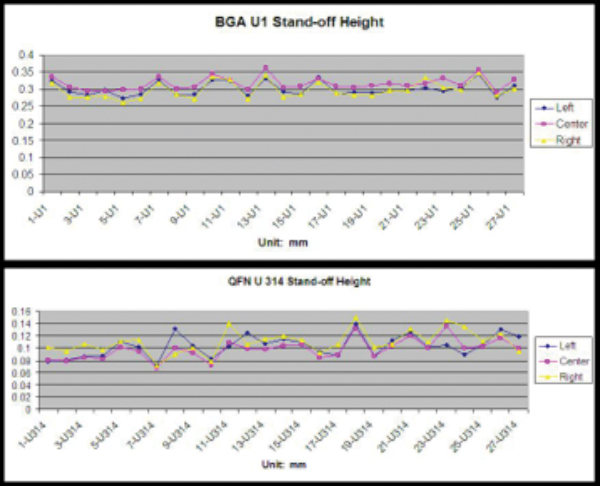
Figure 11. Graph of standoff height on BGA and QFN/BTC.
Summary
New board surface finishes evaluated for this study were plasma finish, ENIS, Hi-P ENIG and ENEPIG. Surface finishes with OSP and IAg were also used. In addition, plasma finish was added as the top coat protection to IAg, Hi-P ENIG and ENEPIG to verify any performance differences.
A total of nine groups of PCB surface finish were evaluated. PCBs were subject to various preconditioning prior to assembly to simulate possible scenarios during typical assembly processes (for example: reflowed in air, baking, misprint, etc). Other preconditioning simulate storage and shelf life, and more preconditioning simulated extreme processes (1x, 2x, 3x reflow prior to assembly). In total, each group of PCB surface finish had 30 pieces available with three samples per preconditioning, except for ENIS where only eight pieces were available.
Based on the results from the solder spread test, there was no significant improvement observed on the surface finish with OSP versus PF, or surface finish with PF added as top coat protection.
On surface finishes with PF, copper discoloration was observed visually and micro-voiding at the pad interface was found on cross-sectioning.
With the results from this study, a rating is provided in Table 2. Hi-P ENIG performs best under fresh conditions, three times reflow, and storage simulation. For fresh conditions, ENEPIG, IAg, and ENIS had better performance than OSP and PF. For three times reflow, Hi-P ENIG, ENEPIG performs better than IAg, ENIS, and OSP, then followed by PF. For storage simulation, ENEPIG performs similarly to Hi-P ENIG, and both are better than IAg, ENIS, and OSP, then followed by PF.
Table 2. Rating Under Select Conditions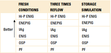
There are many other factors that affect the selection of surface finishes, such as cost, key pad contact, IMC strength for drop/shock/vibration, etc. The user should verify the product design requirement and select the proper surface finish for use.
Ed.: This paper was first published at IPC Apex Expo in March 2014 and is reprinted here with permission of the authors.
References
1. Sven Lamprecht and Petra Backus, “High Phosphorus ENIG – Highest Resistance Against Corrosive Environment,” HKPCA Journal, no. 6, fourth quarter 2002.
2. Y. Oda, M. Kiso, S. Kurosaka, A. Okada, K. Kitajima and S. Hashimoto, A Study of Suitable Palladium and Gold Thickness in ENEPIG Deposits for Lead Free Soldering and Gold Wire Bonding, Uyemura, April 2009.
is operations engineering manager; is director, assembly and test technology; and is vice president engineering, Advanced Engineering Group at Flextronics (flextronics.com); georgie.thein@flextronics.com.


