

2014 Articles
Getting the right temperature is a balancing act, at times requiring fine juggling.
Creating a thermal profile isn’t as straightforward as it once was. PCBs are populated with a growing assortment of new packaging and technologies, introducing new challenges and their associated tradeoffs when it comes to creating the thermal profile. Usually, a conventional board consists of a mix of passive and active components in traditional packaging. Increasingly, boards are populated with µBGAs, µCSPs and µQFNs, as well as the larger BGAs, CSPs, and QFNs. Plus, there is continually smaller packaging like 01005s for passive devices.
Creating a profile for a board like this poses perplexing issues, since larger packages require more heat compared to smaller ones, and there are special considerations when it comes to package-on-package (PoP). Finding a temperature setting that’s acceptable to both larger and smaller packages, while juggling tradeoffs and special considerations, is a balancing act. It’s critical not to overheat smaller packages to avoid solder bridging. On the other hand, more heat needs to be applied to the larger BGA packages for solid solder joints and to keep from creating open solder joints.
After creating the thermal profile, the first-article board is run through reflow to determine whether the profile is good. At this point, x-ray inspection can be performed on both larger and µBGAs to determine whether issues exist: for instance, voids and other defects (Figure 1), such as whether BGA balls have collapsed per IPC standards. That first board informs and defines adjustments needed to the reflow profile.
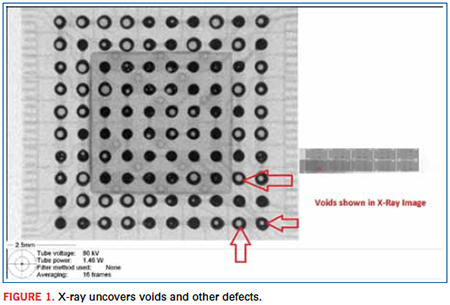
X-ray covers about 90% of the issues the process engineer views as a board goes through reflow. These x-ray visuals provide the roadmap for the type of adjustments that may be needed, such as a shorter or longer soak time or determining whether or not BGA balls aren’t collapsing. Then a higher peak temperature might also be needed for that particular board to reflow properly.
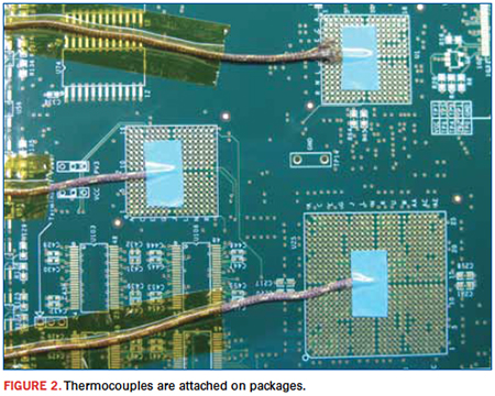
A variety of adjustments can be applied to the profile to accommodate large and small packages. In general, profiling involves making those adjustments on a board-by-board basis. The most common way to establish a profile is to first set a baseline and run it through the oven. To do that is a multi-step task. First, hermocouples are attached on these packages (Figure 2). To set the reflow oven temperature, a reading is taken to show the amount of heat these components
are exposed to when they go through the reflow oven at a certain speed. Once a reading is taken and the board exits the oven, the profile is refined by adjusting the pre-soak, soaking and reflow temperatures.
The right balance must be struck among soak time, peak temperature and reflow time. Soak time is fine-tuned to the critical components. A long soak time is normally not required for smaller packages. Larger packages, however, do need a longer soak time to provide sufficient time for paste flux volatiles to evaporate prior to reflow.
Part of that soak time review is to investigate differences in paste characteristics. These can drive the differences for each profile. Normally, for larger packages, the tendency is to target soldering issues by setting a longer and higher soak time. But at the same time, a lower peak temperature might be needed. This is done to avoid overheating smaller packages.
When profiling, ensure that peak temperatures are reached for the larger mass BGAs, but take care not to burn out the sensitive components. Simultaneously, temperature across the conveyor belt must be taken into account. That temperature can range anywhere from 2° to 5°C. Often, the edges of the PCB represent the coolest areas while in the oven. Therefore, they require even more heat if BGAs are placed on the edges of that particular board. For example, if a BGA on a particular board is normally set at the maximum peak temperature of 245°C, the tendency would be to bump it up. At the same time, however, keep watch on such components as electrolytic capacitors. For instance, by lowering their maximum peak temperature to around 235° or 240°C, that will prevent too much heat from being applied to those smaller components.
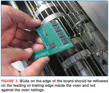
Also, railings on reflow ovens have to be taken into consideration. Temperatures closer to the railings tend to be several degrees cooler than the middle of the oven, thus having a huge impact on the profile. This can make the difference between a good and bad BGA reflow process.
There are several ways to resolve this. One is design and place BGAs away from the edge of the board. Ideally, BGAs will be located closer to the middle of the board. If this is not possible, an alternate approach is to make a reflow fixture for that particular board. The fixture would center the board in the oven to alleviate issues of cooler temperatures toward the edge of the board.
A major profile adjustment for process improvement is to turn that particular board 90° so that the BGAs on the edge of the board are either on the leading or trailing edge inside the oven, not against the railings of the oven (Figure 3).
Leveling the Heat
Take a PCB populated with BGAs, QFNs, CSPs and DFNs. Temperature readings are taken on these particular devices when a profile is being created. The reason is when higher temperature settings are applied on larger components, it’s important to ensure that the smaller components don’t overheat. Applying too much heat causes component failure or causes solder paste to exceed manufacturer’s required temperature readings. Efficiently and strategically spread the thermocouples across the board to achieve as accurate a reading as possible. This includes monitoring the middle and corners of the board.
Failure to achieve the right balance can lead to problems during testing or quality control. Some problems can be solder balls and delamination on the PCB. Solder balls usually occur when the board undergoes an excessive heating rate as it passes through the reflow oven. The reflow cycle is too long, and solder balls form throughout the board. Also, excessive heat can cause board delamination, compromising the reliability of the PCB.
Temperature setting is the trickiest part associated with balancing this trio of profile characteristics. Some components simply cannot handle higher temperatures or are highly heat-sensitive at certain temperatures. In the event a heat-sensitive component is used, the OEM should alert the assembler in advance and advise whether a SnPb or Pb-free profile is desired.
SnPb and Pb-free components are required on a board at times. Processing a Pb-free BGA based on a leaded thermal profile is certain to induce problems. A leaded solder’s melting point is about 25° to 30°C lower in temperature than that of a Pb-free material. In this particular instance, an open ball problem can result from using the wrong thermal profile.
The opposite is also true when processing a leaded board based on a lead-free profile, which requires considerably higher temperature. This mismatch can result in shorts or board warpage. BGA voiding is yet another defect that occurs. This is where the BGA is not 100% collapsed, and a void exists that results from one of multiple and different factors. A common adjustment to minimize voiding is a long, high soak and a lower peak temperature. The longer soak and high temperature is to provide sufficient time for the volatiles in the paste flux to evaporate prior to reflow.
Lack of BGA localized heating is another issue that might be encountered. This means that the BGA is not getting enough heat and the balls are not collapsing. Sometimes the thermal profile is not optimal, thus creating BGA voids. For example, a BGA that is typically heated to a maximum peak of 245°C might see the temperature increase slightly to ensure proper reflow.
PoP Profiles
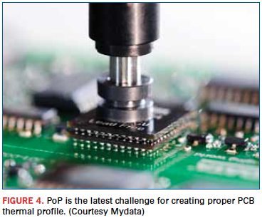
Package-on-package (PoP) poses a new challenge for creating the correct and proper thermal profile for a PCB (Figure 4). In this case, there are certain pros and cons to deal with. As of this writing, there are two popular ways, and either one can be a contract manufacturer’s preference since there is no standard profile for PoP. One involves separately reflowing one component on top of the primary one at the rework station or in the reflow oven. This process is performed before the PoP is installed on the board, and a separate profile is created for that component only. Once the top components are loaded onto the bottom ones using the rework station, all PoPs are installed on the PCB, and the entire board is run through the oven. The assembler needs to consider placement accuracy, paste or flux dipping and reflow warpage as critical areas for PoP applications.
The second method is soldering both components at the same time. In this instance, they are reflowed through the oven together and with the board. That particular profile could be used for every board with similar types of PoP components on that particular assembly. But most important is the level of research performed to achieve the correct profile and the steps taken to create it.
The two methods of PoP soldering have their respective pros and cons. The two methods are rework station and reflow oven. The advantage of using the rework station for PoP is that it targets the heat at one particular area. Nothing else is reflowed on that particular board. Consequently, temperature settings can be adjusted only for that particular area. As far as the engineer is concerned, this is a real plus, since no other parts on the board are affected as the PoP is reflowed onto the board by itself. This process works best mainly for small production runs like prototypes or small runs of five to 10 boards.
The disadvantage is the limited number of rework stations on the assembly floor. Usually, there’s one or two. So, the issue here is meeting delivery schedules since this process is not well suited for large-volume runs, unless multiple rework stations are on the manufacturing floor.
The advantage of using the reflow oven for PoP is the ability to make large-volume quantity runs on the production floor. The disadvantage is the fact that it
profiles the entire board, not just the PoP component. This means all the components on the board must be taken into consideration. And they also go through a thermal cycle.
In this scenario the process engineer encounters different problems in terms of different components handling different temperature levels. Therefore, a profile is necessary for PoP components and other sensitive components such as CSPs, QFNs, and DFNs. In effect, a general idea of a proper profile and defining the right temperature settings represent the key objective here. Here, it’s not so much as trying for a perfect profile, but one that’ll work for a particular board without creating any further issues with any type of package, like BGAs, LGAs, or PoPs.
Simon Ilustre is a process engineer at NexLogic Technologies (nexlogic.com); info@nexlogic.com.
Is there a way to more tightly integrate materials and process development so as to accelerate the pace of innovation?
The electronics supply chain has evolved at a relatively slow pace and there hasn’t been an effective disruption to the operating method in nearly 20 years. The need still exists, however, for original equipment manufacturers (OEMs) to pursue a new way of creating a smarter, faster and better method to speed up the product development lifecycle in order to meet the demands of retailers and consumers. OEMs need a model that enables them to acquire increased control over the lifecycle while leveraging the ingenuity of the supply chain that supports their manufacturing suppliers.
In the past, suppliers have tried – and failed – to adapt the supply chain in order to speed innovation. These methods haven’t fared well in the market for a number of reasons. First, suppliers tried coming at it through a manufacturing approach, typically with a supply focus (either materials or equipment). Through this model, the materials or equipment created for assembling end-product were not always designed in a way where they could be implemented in the manufacturing phase; rather, they were engineered as standalones without taking the bigger picture into account. They failed to address questions such as: How will the solution interact with other aspects of the design? How does this impact the overall design process? What supporting materials, equipment or processes are needed in order to implement the new material? Because not all of these factors were consistently taken into account, OEMs missed out on including the latest technology into their products, and processes and suppliers had excess waste since their technology couldn’t be used.
Another reason some approaches failed is a lack of sufficient global distribution to reach the necessary customers in a timely manner.
Finally, some OEMs did not fully buy into the idea of working directly with a material or equipment supplier – that a design solution was just as valuable as a supply solution.
OEMs by their nature look for solutions that don’t yet exist. Although the EMS supply base has excellent solutions that exist today, and can offer high yield and steadily lower manufacturing costs, the industry as a whole is focused on process development, not product development. So how can we effectively speed innovation on the supply side without repeating the mistakes of the past?
One path forward is to develop and maintain stronger, tighter relationships throughout the supply chain, to collaborate in more efficient ways, and to communicate more effectively. H.B. Fuller’s strategy involves working in the very early stages with the OEM designer to come up with something unique. This angle targets both design services and materials, which is typically how end-customers approach new product generation.
H.B. Fuller’s acquisition of Engent is one step in that direction. This partnership has enhanced our ability to engage OEMs early in the design cycle and support programs at the systems level. The emerging technology required for the new product is developed by working closely with the OEM, typically on multiple continents, and with the OEM’s manufacturing partner. When the product is ready to receive the green light for full-scale production, H.B. Fuller deploys resources directly at the final manufacturing site, ensuring process support and a quality ramp-up of product manufacturing. This type of partnership streamlines the process for all parties involved in the supply chain. By leveraging Engent’s expertise in next-generation electronics manufacturing and technology services, as well as utilizing our own large-scale connections in the supply chain and global distribution capabilities, H.B. Fuller makes it possible for OEMs and suppliers to have a single source when it comes to global testing and developing. And by gathering all members of the supply chain in one place, improved communication and collaboration happens.
This new electronics supply model represents a shift in terms of how members of the supply chain interact and move products from concept to consumer. While the traditional model has suppliers mainly working at the manufacturing level – meaning they are focused on developing new equipment or materials – and are mostly independent of OEMs, this new approach emphasizes the entire supply chain coming together to work at the design (or “systems”) level. This is a significant divergence from the old model, where suppliers would develop groundbreaking new equipment or materials, but later learned that the assembler might not have the facilities or capabilities to use them in manufacturing lines.
Here’s how the new model works: OEMs present design challenges that are defined at the systems level. By having all members of the supply chain working jointly to solve these challenges instead of in silos, the supply chain is forced to expand its knowledge past what they sell. This gives OEMs the ability to speak at the systems level to the supply chain, thus speeding innovation and production processes through increased information transfer and better communication. In theory, this is just an ideal. To achieve it, the supply chain must interact both collectively and as independent groups within itself – from materials, components and adhesives to PCBs, manufacturing equipment, etc. In addition, all parties must act interdependently in the supply chain and attempt to proactively innovate on the OEM’s behalf. The knowledge gained and shared through working interdependently helps create a more efficient model for innovation because all parties are collectively designing products and materials, rather than just OEMs or suppliers.
Working together at the design level rather than the equipment or material level allows compatible OEMs, material suppliers and the rest of the supply chain to be more acutely aware of each other’s projects and ideas. This leads to improved collaboration, which in turn speeds the development and innovation process, satisfying both the OEMs’ and consumers’ needs. In short, all members of the supply chain work in concert to discuss and develop new design solutions. This method enables OEMs to achieve streamlined innovation, while suppliers use their increased access to OEMs to develop solutions they know the EMSs have the capacity to manufacture.
This new approach helps supply chain parties become smarter about how to structure their business operations in efforts to better collaborate and communicate with one another. Each member in the supply chain must learn how to best interact with each other and share crucial information to help optimize the production process in the changing electronics manufacturing world.
H.B. Fuller is executing this strategy through its partnership with Engent, an Atlanta-based electronics process development company. Why Engent? While many smaller EMS companies take and implement tried-and-true processes developed elsewhere, Engent develops these processes in-house. Starting as an advanced process group and eventually spinning out of Siemens in 2002 as a standalone business, Engent now has several capabilities unique for a company its size, especially in the area of leading-edge packaging, such as multichip module (MCM), chip-on-board (CoB) and MEMS.
H.B. Fuller’s hierarchy, then, includes three parts: an advanced chemistry group that focuses on developing polymer platforms and longer-term programs; a product development group focused on customer needs of today; and Engent, which will work on next-generation processes, applications development for ideas that are roughly three years out.
New Benefits, New Demands
With the new model come many benefits, but there are also demands as well. OEMs are starting to challenge the supply chain and ask what it can do to help them innovate quicker. They want partners who have knowledge that encompasses more than just what they sell and who can offer facilities that incubate the development of technology, as well as onsite production support.
Using this method, H.B. Fuller in partnership with Engent helps provide these benefits to all involved in the process. We are looking to streamline the production process upfront for OEMs and fully leverage suppliers’ and the supply chain’s intense knowledge and infrastructure. And we are approaching the supply chain in a way that focuses on solving problems at the system/design level rather than the traditional method of suppliers selling a specific material or equipment.
This model represents an efficient method for developing products and speeding innovation, and it offers benefits at every level of the supply chain. OEMs get the innovation and help from the supply chain they need to keep pace with consumer demand and will also enjoy better advancements in technology for their products in a compressed timeframe, providing a competitive advantage in one of the most highly competitive marketplaces. Suppliers achieve maximized yields and are more involved in the innovation process – being proactive instead of reactive. And the rest of the supply chain benefits from their increased access to communication lines with OEMs.
While we believe this strategy will work for H.B. Fuller, the likelihood of it becoming the standard model is small, but there are reasons for that. It is a model better suited for materials suppliers than for capital equipment manufacturers. Assemblers tend to prefer common equipment in order to avoid having to train employees and support multiple equipment sets. When it comes to materials though, most customers want choices. The materials business is not binary. Even when a supplier doesn’t “win” a program, it tends to get some of it.
Companies with both Engent’s size and technical capability are hard to find. Materials companies as a rule don’t invest in EMS capabilities, as running a service-heavy business is not necessarily a core competency. In addition, most materials suppliers invest where there’s promise of future volume. This approach is not always going to result in a new and widely used technology.
But the new model does resonate with some OEMs, as key players see a need for early stage design capability. Even if there’s no guarantee that a new, highly commercial material will be developed, H.B. Fuller’s success will be measured on whether we continually develop our knowledge base and increase the pace of innovation.
Matt Perry is the director of North America business development, electronic materials at Engent (engentatt.com); matt.perry@engentaat.com. Zhiwei Cai is director of electronic and assembly materials at H.B. Fuller (hbfuller.com).

Optimized, automated material replenishment can significantly cut solder waste.
If there’s one certainty in the print process, it’s that you have to have paste in front of the blade to print. Seems obvious, I know, but I could tell you countless tales of board defects, line stoppages and low yields because of insufficient solder paste in front of the squeegee blade. And, while it seems easy enough, in a high-volume manufacturing environment that’s producing assemblies with highly miniaturized devices, ensuring consistent volumes of paste in front of the squeegee is essential to high yields and optimized throughput.
What I’ve observed on many occasions is an operator who manually puts down a tremendous amount of solder paste so that it will last the entire shift. This approach might be sufficient in an operation that is fairly low volume and is assembling standard SMT boards. If, however, one is printing at a higher level with more miniaturized devices, more complex circuitry and geometries in high volume, having the correct quantity of paste in front of the blade is critical. Without it, print quality and, therefore, yield levels are affected.
The other factor to consider is the impact the environment is having on the solder paste. Laying down an entire jar of solder paste at the beginning of the shift may certainly lend itself to unintended consequences. With a material that is potentially changing with environmental exposure (i.e., the material may be susceptible to moisture; solvents could be pulled out by the atmosphere, etc.), the dynamics of the print can be upset. So, not only is it ideal to have the correct volume of paste in front of the blade, but the correct volume of fresh paste.
Automating paste deposition is the most effective method to ensure proper volumes of new, fresh material is placed in front of the squeegee blade. Most printing equipment manufacturers have such tools, and they are worth the investment. Automatic paste deposition technology can be combined with a paste roll height monitor for completely automated, hands-off, quality paste management. The paste roll height monitor functions just as the name implies; it uses a vertical laser to detect paste presence and roll height sensing, which saves significant operator monitoring and application time. Closed-loop paste level detection provides alerts for either manual or automatic paste replenishment and, therefore, avoids insufficient paste deposits and down-the-line defects. According to our company’s test data, combining the paste roll sensing functionality with automatic paste dispensing has numerous benefits, particularly in high-volume operations. Operator intervention is significantly reduced and can result in downtime savings of up to 40 min. per day. When your printer is churning out over 2,000 boards per day, that can result in tremendous throughput improvements.
Optimized, automated material replenishment has also been shown to reduce paste outside the print area by 80%, and solder paste wastage is significantly reduced, saving as much as 100g per day. In addition to the cost benefits from limiting paste wastage, perhaps the most significant benefits are defect reduction and process control improvements. When the volume of paste in front of the blade is inconsistent from side to side – particularly with smaller, high-density apertures – there will be defects. In fact, data from one of our customers showed that there were 685 defective parts per million (DPPM) fewer when using automatic paste replenishment. Finally, Cp and Cpk also showed substantive improvement when using the combination of paste roll height sensing and automatic paste replenishment. The Cp moved from 2.19 without these technologies to 2.57 with them, and the Cpk increased from 1.8 to 2.34 when the systems were incorporated.
At the end of the day, when variables are removed from the printing process, the better the results will be. Less operator intervention generally equates to more effective process control. Such is the case with machine-controlled paste roll height monitoring and automatic paste dispensing. The combination of these two technologies improves throughput, reduces material waste, dramatically increases yield and raises quality levels significantly. With an ROI payback of less than one year, it’s a quality investment worth making.
Clive Ashmore is global applied process engineering manager at DEK International (dek.com); cashmore@dek.com. His column appears bimonthly.

Press Releases
- The SearchWorks Group Shares Mid-Year Read on the EMS Talent Market
- Altus Announces Return of ‘Factory of the Future’ for 2026
- Circuit Technology Center, Inc. Expands High-Volume BGA Reballing Capacity with Investment in Additional Reflow Oven
- SEMI And Global Net Corp. Release New Report On Glass Core Substrate Market And Development Trends For Semiconductors