

2013 Articles
The five-year forecast calls for 38% growth, driven by the industrial and communications sectors.
The electronics manufacturing market is big; global assembly of printed circuit boards exceeded $1 trillion last year. Given such a vast marketplace, there are numerous opportunities for companies to specialize in one or another technology. Embedded computing is one such technology with a great deal of promise.
The merchant embedded computing (MEC) market is a specialized market within electronics assembly. It is a dynamic industry, with advances occurring continuously, thanks to an energetic standards development effort. MEC modules and components are board-level computing systems and solutions, based on specifications controlled by a dozen or so standards organizations that have grown up along with the industry. Literally hundreds of standards – adopted or still under development – are controlling the design and manufacture of embedded applications. Also, more than 200 companies worldwide are developing and manufacturing products, with an additional 100 to 200 participating in the distribution and assembly of embedded computing boards and their components.
New Venture Research has been tracking the merchant embedding computing market for over 15 years. In our latest report, the Merchant Embedded Computing Market – 2013 Edition, we provide a historical analysis and forecasts of the embedded computing market, as well as our observations of market trends for the coming five years. Data are based on field-user surveys and interviews by industry participants, as well as our other reports related to electronics assembly. We analyze the overall market from three separate, but interrelated, perspectives:
- Applications: five application segments targeted by MEC companies.
- Bus architectures: nine categories, based on the bus architecture and form factors of embedded boards and modules.
- Board function: four functional design categories of board-level products.
Sadly, any current analysis of today’s electronics marketplace must start with the recession of 2009 – a near-economic calamity often compared to the Great Depression of the 1930s. The recession left an indelible mark on virtually every aspect of the global economy, not least the electronics assembly markets, including the market for embedded computing. Figure 1 shows the impact of the economic downturn on the MEC industry. In 2009, there was an abrupt and significant reversal in the growth rate, as well as total revenues of the MEC market. The pain was felt in virtually every segment of the MEC market. Yet, seen from a wider perspective, the “Great Recession” was little more than a blip in a history of consistent growth by the industry. Despite the severity of the downturn, by 2012 the market had fully recovered in terms of total market size, and seemingly in momentum. Moreover, the MEC market is projected to continue growing well into the future, according to our research.

One reason for our optimism is based on the nature of the MEC industry. Thanks to the evolution of old standards into new, and more advanced ones, the manufacturers of embedded computing modules and components are constantly working at the leading-edge of technology, providing products that ultimately save customers money. Ivan Straznicky, a technical fellow at Curtiss-Wright Controls Defense Systems, a long-time player in the merchant embedded computing market, points out that today’s merchant vendors can take advantage of the opportunity of “relieving the pain of our customers.” According to Straznicky, “Whereas in the past, they would have been tempted to build these components themselves, they now come to us because we have ready-made solutions that have been developed across multiple customers and been field-proven.” This is both the benefit and the promise of embedded computing.
Positive trends. A number of market trends point toward a growing MEC market, including:
- Purchasing by large sectors of the economy has picked up for MEC products, as telecommunications companies, industrial automation companies and government (particularly in the defense industry) are spending on repairing and replacing equipment that depend on embedded computing devices. Such maintenance work all but stopped during the recession, so pent-up demand is helping drive the market.
- The transition toward digital communications, as well as skyrocketing traffic, is driving telecommunications carriers to rapidly upgrade their networks and private enterprise to increasingly move toward IP and data communications products. The MEC industry is well placed to take advantage of this transition.
- Next-generation, high-integration silicon is enabling manufacturers to design board-level systems with capabilities not possible even five or six years ago. Improvements include lower energy consumption and very high-speed serial bus interconnects, all within small form factors. Embedded computing vendors are tightly focused on leading-edge technologies and board architectures, which will place them at the forefront of emerging markets in the coming years.
Microprocessor manufacturers, particularly Intel, continue to raise the bar with ever greater integration and more powerful chips, and as Jim Renehan, director of marketing at Gainesville, GA-based Trenton Systems points out, there is a need among standards to move up the “food-chain” to provide more capability for boards and plug-in cards.
MEC vendors face competition from other electronics sectors, as well, including the electronics manufacturing services industry. (NVR tracks the EMS market in a companion report, The Worldwide Electronics Manufacturing Services Market.) Both industries depend on sales to OEMs and to government prime contractors. EMS vendors have an advantage in selling products in large numbers at low cost. Many MEC vendors, on the other hand, are small and specialized in niche markets. Their products are, by nature, customized and sold in small quantities. But the rewards in such a business model can be high, as the vendors can act quickly and build to specifications not possible by EMS competitors.
Some segments of the MEC industry have fared better than others as the market has emerged from the downturn, and in the following sections, we analyze the issues and opportunities for each of the major market sectors covered by our report.
Application markets. The MEC market consists of four leading application markets – communications, industrial automation, medical, and military/aerospace – and an “other” category that includes a number of vertical markets, such as transportation, security, surveillance, point-of-sale/kiosk applications, etc.
These application markets tend to have very specific product requirements that differentiate them from one another, as well as from other electronics assembly market segments such as PCs and the general purpose embedded electronics markets. Requirements include operating in harsh environmental conditions of temperature, humidity or vibration; greater reliability and security; and specific real-time computing functionality. Hence, the market leaders, competitive forces, growth rates and size of the different application segments vary widely.
Figure 2 presents a top-level analysis of the MEC market from the point of view of the five application market segments for 2012. Prior to the industry downturn, the communications application market was the largest single market segment. However, general industrial automation applications have made a stronger comeback than has been seen in the telecommunications sector and, by 2012, had become the largest and fastest growing MEC market.

The growth of the industrial automation application market – “Big Data,” as Renehan refers to it – is at least partially a function of corporations around the world upgrading their circa-2007 systems with new energy-efficient systems. It is claimed that these new technologies can enable users to replace 10 servers with one new multicore server and permit an energy payback in fewer than 18 months. Other advances include large increases in the ability to move massive amounts of data in and out of systems, requiring interconnect speeds to grow from 1Gbps today to 10 and 40Gbps. This is good news for MEC communication suppliers, as well as industrial manufacturers.
Over the next five years, we expect this trend to continue. While the communications application market will grow at a pace equal with the overall market, industrial automation products will outpace communications, and will account for more than one-third of the total market by 2017.
Medical applications was also hit hard by the financial crisis, which slowed MEC-based purchases of large equipment considerably. Unlike other manufacturing sectors, which have begun to replace and upgrade equipment, new spending in the medical segment is still depressed, in part due to uncertainty in the US about forthcoming changes in the national healthcare system. Consequently, we do not expect this market to grow as quickly as other segments.
Military and aerospace applications suffered in much the same way as industrial automation. And it has rebounded for much the same reason. NVR expects that various challenges of providing to the mil/aero market will slow its growth rate, somewhat. Growth in this market is closely tied to politics and to the security issues facing all defense-related markets, and these challenges will impact short-term growth rates.
Even so, Michael Macpherson, vice president of strategic planning at Curtiss-Wright, points out that, overall, the global picture for this market segment looks quite healthy. Curtiss-Wright is a leading competitor in the military and aerospace market segment. From Macpherson’s point of view, the market constraints have been primarily in the US. He specifically points to the debates over the budget and sequestration as having put pressure on the “topline of the defense market.” As a consequence, there may not be quite as many of the multi-billion-dollar programs. “But we do the electronics,” Macpherson notes. “And while there may not be as many new, big programs, the fact that they are still upgrading and doing service life extension for existing platforms means they are still upgrading the electronics, and that is good for us.”
Rodger Hosking, a vice president and cofounder of Pentek, a New Jersey-based merchant embedded computing vendor that also focuses on government and military markets, agrees. One of the drivers of this market, he points out, is that government organizations are faced with maintenance costs of older systems that can be replaced by newer systems with “one tenth of the cost, one tenth the power dissipation and one hundred times the performance. So, you look at the economics, as well as the strategic advantages of some new technology, and it’s quite a simple equation for a government electronics customer to justify upgrading or replacing older equipment.”
Bus architecture markets. Market penetration by the various embedded computing bus architectures is driven as much by technology as it is by market forces. The nine bus architecture categories defined in our report are as follows:
- PCI.
- CompactPCI.
- AdvancedTCA (ATCA).
- VMEbus.
- PMC.
- AdvancedMC (AMC) and MicroTCA.
- PC/104 and its variants, plus EPIC, EBX and motherboards (ATX and ITX).
- COM and COM Express.
- Other.
Each MEC bus architecture has a different rate of adoption depending on the needs of individual application segments. Some are older parallel-bus technologies and nearing their end-of-life, as is the case for PCI-based buses, specifically the PCI and CompactPCI architectures. CompactPCI (cPCI) has historically captured the largest share of the MEC market, but this is changing, as PCI architecture market shares are rapidly shrinking. Figure 3 shows that cPCI was the largest single bus architecture segment in 2012. NVR expects that within two years, its market share will drop below that of VMEbus – however, not necessarily owing to any great growth by the latter segment. Also, an “old” bus architecture, VMEbus standards and products have changed and adapted to the advances in technology and consequently will remain a significant product segment. Helping VMEbus products stay competitive is the fact that this architecture is specifically designed for extreme environments, a design feature that makes this an ideal product for many industrial automation applications, especially for mil/aero applications.

Yet, VMEbus will grow only more or less equally to the overall market, while the big winners for the future are products driving the industry toward higher integration in smaller form factors. This trend is reflected in the growth rates of the computer-on-module (COM) bus architecture. This technology will grow at double-digit rates between 2012 and 2017, largely because it is enabling vendors to create complete systems on a highly integrated single board. PC/104 and its variants are also small form factor architectures, but are not as trendy as COM.
Looking to the future, though, if you had to describe the most significant trend in the evolution of MEC architectures, it can be pared down to a single word: “Faster,” says Todd Wynia, VP of planning and development at Emerson Network Power Embedded Computing. “The industry has shifted from bus-based architectures to a fabric-based industry,” he says. “Instead of being the VMEbus or compactPCI of the past, it’s now Ethernet-based backplanes for architectures like ATCA or the evolution of compactPCI or VPX – all fabric-based interfaces. And the evolution of those interfaces is ever-faster.”
In keeping with that evolution, we expect to see a rapid expansion of AdvancedTCA, as well as AdvancedMC bus architectures. Both of these form factors were originally developed for telecommunications, but they have since expanded into industrial automation markets and are consequently experiencing high growth rates. AdvancedMC is particularly worth watching. The AMC specification was only adopted in 2005, yet we expect that it will capture nearly 8% of the total MEC market by 2017.
New bus structures are continuously being developed by merchant vendors. Basing their design and manufacturing on existing standards and on new specifications being developed by the standards organizations, the vendors sell a bewildering array of off-the-shelf embedded board designs to OEMs and even end-users. Moreover, most companies are willing to develop custom architectures based on existing product lines. This constant innovation serves to strengthen the MEC industry and at the same time fend off competition from EMS vendors. High volume is not necessarily the name of this game; rather it is innovation, customization and optimization that will drive the MEC market through the next decade.
Board function markets. The MEC industry can also be categorized according to the functional design of embedded boards. NVR identifies four board function categories: single-board computers (SBCs), digital signal processor boards (DSPs), I/O boards, and other board functions. The last category incorporates a huge number of diverse and specific functions, many of which are custom designs, including switchboards, chassis, backplanes, and system integration devices. The MEC board function markets are presented in Figure 4, providing market share of each functional category for 2012.

In some applications, I/O boards are proliferating and are customized to the wide spectrum of I/O functions that different applications use. Other board functions are also proliferating, mostly owing to a growing demand for custom products. But the real story for MEC board functions is a persistent shift toward single board computers. MEC vendors are more and more integrating all of the electronic components and functionality into SBCs, creating complete systems. (This trend goes hand in hand with the growth of COM bus architecture, which is, by definition, a SBC board function.) Leading manufacturers like GE Intelligent Platforms exemplify this trend. GE considers single board computers as increasingly significant for its product line. According to Ian McMurray, speaking for the embedded computing group, SBCs are at the heart of its military/aerospace business, incorporating an extensive range of component products, including microprocessors, sensor processing systems, video processing platforms, image processing technology and highly rugged routers and switches.
Increasing integration onto the SBC platform has always been a characteristic of this market segment, and it goes hand-in-hand with the evolution of bus architecture technology. The key elements driving this trend – processors, fabrics and integration – are leading increasingly toward advanced fabric-centric architectures, such as VPX, which McMurray notes has become the architecture of choice for new military programs at GE Intelligent Platforms. Moreover, as SBCs integrate and incorporate ever more of digital signal processing, graphics and I/O functionality, the need for separate DSPs and I/O boards decreases, and leads to growing demand for single board products like the COM Express form factor. Thus, already accounting for more than half the total MEC market in 2012, NVR projects that the SBC market segment will continue to expand its market share of the total MEC market over the next five years and beyond.
Conclusions
Throughout this discussion, we have touched only lightly on the thing that gives meaning to the merchant embedded computing market: the active, dynamic standards process. Despite a bewildering array of products and designs, the products that drive the MEC market are themselves driven by relatively few organizations that bring together (sometimes fierce) competitors to work collectively to develop open specifications that help everyone – manufacturers and customers alike. From the earliest consortia – such as VITA, PCI-SIG and PICMG – to the most recent – SFF-SIG and SGeT – these organizations empower manufacturers to concentrate, not on basic form factors and connectors, but on building the best mousetrap for the application.
Significant changes are happening in the MEC marketplace and in the electronics industry in general. Along with the evolution of technologies, such as the shift from parallel to serial and from simple buses to fabric-based architectures, the standards organizations are constantly evolving their standards to keep pace. As Moore’s Law continues to be demonstrated by ever more powerful chips, applications once needing discrete chips for separate tasks are being integrated into single, more densely packed chips, and new standards specifications will make it possible to integrate those chips into embedded designs. The challenges raised by decreasing size and increasing performance cannot effectively be addressed by individual companies. It is the PICMGs, VITAs and SFF-SIGs that will help speed these trends. It is these organizations that are helping define the future of embedded computing by advancing the technologies incorporated in standards specifications.
These trends are altering the MEC board market at an accelerated pace. Not only will much of today’s separate chip functionality get subsumed into a single chip design, but also the computational power and functionality of single-board computers will skyrocket. “There are always challenges to overcome,” concludes Rodger Hosking of Pentek. “That’s what keeps us in business, and it’s what keeps the industry going. The big driver is the silicon and component technology. Everything that we are surrounded by – the electronics in our cars, mobile electronics, everything – is getting more powerful, smaller, less expensive.”
Jerry Watkins is a senior analyst with New Venture Research and author of numerous syndicated reports in the telecommunications sector and more recently in the computing and merchant embedded computing industry; info@newventureresearch.com.
A 95% first-pass yield is the litmus test. Here’s how to get there.
Capital spending is an internal issue EMS providers constantly grapple with. At the back of the minds of the decision-makers are a host of related and nagging questions. Can we make do with existing equipment? What are our tradeoffs? Will we lose money using older assembly equipment? How will customers perceive older equipment? Can we satisfactorily deliver to OEMs with cutting-edge technologies?
Of all the associated capex questions, the most prominent should be: Do we provide the right levels of technology, manufacturing equipment and expertise to deliver the best product to the OEM?
One way to get there is through sophisticated automated optical inspection systems. The extraordinarily small component packaging and ever-shrinking PCB sizes require superior inspection solutions to detect assembly flaws and defects.
AOI is well-suited for checking tombstones, misaligned or missing components, wrong polarity, wrong parts, lifted leads, and lifted lead banks. AOI ensures that installed components are the right ones in terms of value and footprint. It also catches marginal opens, in which the assembled joint is minimal and certainly not 100%. In many cases, when the AOI operator manually presses on the joint in question, the connection is made.
When older AOI technology is used on the assembly floor, it often is in conjunction with testing, and the latter is expected to catch those latent defects that slip past AOI. A better process, however, is to upgrade the AOI machines. New features include advanced LED lighting, the color of that lighting, camera location, lens resolution, user interface, and better, more comprehensive algorithms for detecting components and flaws.
Beyond the equipment itself, the AOI operator or programmer plays an equally important role. AOI is designed to detect questionable components. However, it’s up to the operator to ensure defects are either “true” or “false.” One aspect they must be mindful of is defining the tolerance or pass code as tightly as possible for defining the right window for reading components on a PCB. Within this tweaking process, if the tolerance window is too tight, it can be increased. But if the region of interest is made too big, then the AOI passes virtually everything, and true faults will be missed.
The experienced AOI programmer will program the right part type, and accurately program the tolerance or pass code. In this second step, the operator performs program tweaking to train the AOI for the right component, as well as define the tolerances, the footprint, size of the rectangle, and the overall region of interest.
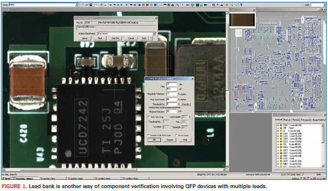
Figure 1 shows the lead bank indication on the AOI monitor. It is yet another way of component verification involving QFPs that have multiple leads. In this case, highly complex algorithms are put to use to inspect these particular components. These lead bank windows are larger in size to not only perform component verification, but also expedite the inspection process.
Compared to the earlier incandescent AOI lighting systems, LED technology has provided AOI operators superior brightness and a clearer, sharper focus on devices and hard-to-see board areas. Also, LED lighting spreads out the viewing area more uniformly to track down flaws and defects in the subject target or “region of interest.” Another advantage LEDs offer is the availability of different colors.
The color white is traditional. But LEDs allow the application of different color filters such as blue, red or an RGB (red, green, blue) option. These filters are especially valuable to improve visibility on small or overly shiny components.
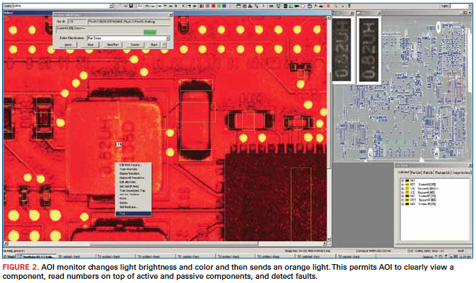
For example, a traditional white light immediately reflects off a glass-based package in the region of interest, creates a blank, and prevents the viewing of that component. Using advanced AOI features, the operator applies the different filters during programming or simply applies the different color lighting if already programmed. Figure 2 illustrates such a case where AOI changes light brightness and color and then sends an orange light. This permits the AOI to clearly view a component, read numbers on top of active and passive components, and detect faults.
As for camera locations, an effective AOI has five different viewing sites. One is on the left, another on the right, the third on the front, another on the back and one on top. This way, a board is captured from every angle. If component markings cannot be viewed from the top, the operator has the option of going to the side angle for a different view and the ability to detect that component. Having different cameras at different locations is a great help in determining and detecting true failures compared to false failures. A greater number of cameras offer better visibility on different sides and different angles with greater depth of field, giving greater coverage of the region of interest. Consequently, true and false faults are clearly seen with no visual ambiguities.
Newer AOI technologies have also introduced higher camera lens resolution. Today’s state-of-the-art AOI cameras sport 25MP. Five years ago, AOI featured 1MP cameras. The big jump in megapixels is providing considerable capability for component feature recognition and a much clearer view. These extra megapixels hand the operator a highly consistent and crisp picture of extremely small areas on top of components. These viewing advances come at a time when such passives as 0402, 0201 and now 01005 are so small that the human eye can barely see them. But with this large number of pixels, they can be clearly spotted.
Two other complementary features are zoom capability and depth of field. Particularly for extraordinarily small component packaging and tight PCB areas, the newer cameras can zoom in from 50 to 250X to closely view those shrinking board areas. Meanwhile, depth of field spreads out the region of interest and makes it considerably sharper to clearly view and locate any possible flaws.
User Interface and Algorithms
The effectiveness of an AOI user interface and the comprehensiveness of its supporting algorithms are synonymous. Operators and technicians solely depend on their AOI’s visual images of the good and bad components or the true or false nature of the devices under inspection. Generally, those are the most effective AOIs today since those are the ones that catch considerably more true versus false faults.
In particular, considerable concentration and effort go into developing and writing the supporting AOI algorithms. In effect, the way this software is written determines how well – percentage-wise – images can be seen and located. The quality of the algorithm can determine whether suspect images are caught by a few percentage points or by a big number. This also means the comprehensiveness of these algorithms must capture images, not only the black and white, but also all the shades of gray in-between or those faults in a “maybe” category.
Those gray areas are becoming more troublesome these days due to shrinking PCB sizes and component packaging, which have generally shrunk 30 to 40% and maybe even more in the past five years. That means smaller packages have a smaller space on which to write with extremely fine type nomenclatures and numbers or the component manufacturer’s name and logo.
Also, it’s important to note that some components today are laser-marked on the sides. In cases like these, a robust algorithm is able to not only shine the light on the side of the component, but also to accurately determine the nomenclatures or numbering laser-etched on the side. Sometimes these laser etchings may not be completely visible with a regular AOI camera. But advanced AOI can certainly capture these faults.
Results obtained through AOI show the levels of first-pass yields achieved. State-of-the-art AOI can detect 99.5% of component faults and failures. Older AOI technology, on the other hand, detects perhaps 80 to 85% of the defects. The question, then, for the assembler, is: What is the value of this additional 12 to 15% detection rate that seriously affects first-pass yields?
A 95% or higher first-pass yield provides the litmus test. OEMs of some end-products demand considerable quality and reliability from the outset. Others might get by with older technology. If defects and flaws aren’t caught at the AOI stage, the PCBs carrying those problems undergo visual inspection or functional test. PCBs aren’t 100% testable. Thus, it’s possible a bad component might slip through AOI and go undetected to the field, especially if the module with the bad component doesn’t undergo testing. Advanced AOI largely eliminates inconsistent visual inspection and reduces dependency on functional testing to ensure defects and flaws are caught early on.
Zulki Khan is president and founder of NexLogic Technologies; zulki@nexlogic.com.
How a novel high-yield package cut costs by 32% vs. COB.
Physicists explore the fundamental constituents of matter by accelerating subatomic particles to speeds approaching that of light and colliding them head on or against stationary targets. The reaction products are then observed in various types of detectors. Recent experimental results from the CERN accelerator facility in Switzerland revealing the long-sought Higgs boson have been widely publicized. Researchers there, and at accelerators elsewhere, investigate the particles produced in such collisions.
The particles produced in these collisions are often bent by powerful electromagnets surrounding the detectors in order to determine the particle charge and momenta. The detectors incorporate tracking devices that capture faint electrical signals the particles produce during their transit. Various types of tracking devices are employed among the experiments at the different facilities, but many of them have in common a readout chip, the APV25, whose basic design was jointly developed for trackers at CERN nearly 20 years ago by a British university and a national laboratory.
The APV25 has 128 analog inputs that each connect directly to a tracker channel. The input signals are amplified and shaped, then sampled, and the results are fed into a pipeline of programmable length. The conditioned signals are read out after receiving a trigger request, further amplified, and multiplexed such that the signals from all 128 channels can be read out on a single line that has a differential current output.
The Compact Muon Solenoid is one of four detectors at CERN and one of two that identified the Higgs boson. Its tracker system has approximately 10,000,000 channels, which are read by the 128-channel APV25 chips (about 75,000 of them). The CMS tracker contains many concentric layers of sensors surrounding the interaction point. The APV25 sensors are wire-bonded directly to PCBs and encapsulated, not packaged, because the mass of a package could compromise particle detection in succeeding outer layers.
The wire-bonded, chip-on-board construction, though unavoidable in the CMS detector at CERN, is inconvenient. Board rework is impractical to replace a failed device; instead, the entire readout board would be replaced, even though the other devices on board are good. However, in some trackers at other facilities, detection would not be hampered if the APV25 readout chips were packaged. Such is the case at the Brookhaven National Laboratory Relativistic Heavy Ion Collider (RHIC) in Long Island, NY, for example.
Bates Research and Engineering Center at Massachusetts Institute of Technology was engaged by the Brookhaven laboratory to design readout electronics for an upgrade to the detector system of the STAR experiment at the RHIC (sidebar). Bates is part of MIT’s Lab for Nuclear Science. It is an engineering facility that designs and constructs instruments for physics experiments in support of work by MIT faculty and other researchers. The initial prototype readout module for the STAR tracker ganged five APV25 chips wire-bonded directly to a printed circuit board. The first prototype module was a composite of two boards laminated together, which distributed the chips’ inputs via bond wires to edge connectors. It was very expensive to fabricate and assemble, and permitted no rework once a chip was bonded to the board.
To reduce the cost of the module, enable the readout chips to be tested immediately before installation, permit rework, and simplify the application of the APV25 to other projects, Bates developed a BGA package for the die and redesigned the readout module. For tracker architectures in which the BGA mass would not interfere with particle detection, the approach greatly simplifies the design, assembly, and maintenance of readout cards.
The BGA package that Bates developed for the APV25 has 315 SnPb solder balls on a 0.8-mm pitch and measures 15 x 20mm. Of the 315 balls, 39 provide only mechanical support and have no electrical function. The package substrate is a four-layer design with 50µm trace width and spacing, using Nelco 4000-29 material (Figure 1). All the slow controls, the clock, the trigger, and the chip analog outputs were routed to one edge of the BGA; the 128 tracker inputs are on the opposite long edge of the package, no more than four balls deep from the edge, with some wrap around. The layout enables routing to all the input channels using only two signal layers on host readout boards. A grid of 9 x 9 balls directly under the die corresponds with a grid of vias connected to the die attach pad for excellent thermal conduction and electrical contact to the negative power plane in the tracker module (Figure 2). Sierra Circuits fabricated the BGA substrates, as well as the boards for the tracker modules, which each monitor 640 channels (Figure 3).


The packages were assembled with known-good die, which were bonded with 25µm gold wire and encapsulated. A test board with a custom BGA test socket was used to evaluate the basic functionality of the assembled APV25 devices. A 94% yield was achieved.
It is helpful to compare the costs to produce 80 tracker modules of the chip-on-board design and 80 tracker modules with the BGAs. Including NRE, that many chip-on-board tracker modules would cost more than $65,000, versus slightly less than $44,000 for the BGA version, including NRE.
The Physics of RHIC
The Relativistic Heavy Ion Collider primarily collides ions of gold, one of the heaviest common elements, because the gold nucleus is densely packed with particles. The ions are atoms of gold that have been stripped of their outer cloud of electrons.
Two beams of gold ions are collided head-on when they have reached nearly the speed of light (what physicists refer to as relativistic speeds). The beams travel in opposite directions around the facility’s 2.4-mile, two-lane accelerator and at six intersections the lanes cross, leading to an intersection.
If conditions are right, the collision “melts” the protons and neutrons and, for a brief instant, liberates their constituent quarks and gluons. Just after the collision, thousands more particles form as the area cools. Each of those particles provides a clue about what occurred inside the collision zone.
Physicists had postulated that all protons and neutrons are made up of three quarks, along with the gluons that bind them together. Theory holds that for a brief time at the beginning of the universe there were no protons and neutrons, only free quarks and gluons. However, as the universe expanded and cooled, the quarks and gluons bound together and remained inseparable. The RHIC is the first instrument that can, in essence, take us back in time to see how matter behaved at the start of the universe.
Brookhaven National Laboratory announced in 2010 that the RHIC had produced the highest temperature ever recorded (4 trillion degrees Celsius, roughly 250,000 times hotter than the core of the Sun), thus recreating an exotic form of matter that had not existed since microseconds after the Big Bang. Researchers for the first time were able to positively confirm the creation of the quark-gluon plasma. For less than a billionth of a trillionth of a second, quarks and gluons flowed freely in a frictionless fluid that hadn’t existed for 13.7 billion years.
Benjamin Buck is an electronics engineer at MIT Bates Research and Engineering Center and designer of the BGA package and associated electronics for the STAR experiment at the Relativistic Heavy Ion Collider at Brookhaven National Laboratory; bbuck@mit.edu.

Press Releases
- IDTechEx Report Unveils 3D Electronics Status and Opportunities
- Hon Hai Technology Group (Foxconn) Pledges 100% Renewable Electricity By 2040 and Joins RE100
- ZESTRON Academy Introduces Cutting-Edge SMT Webinar Series for 2024
- AIM to Highlight NC259FPA Ultrafine No Clean Solder Paste at SMTA Juarez Expo & Tech Forum